
Инструмент проще, чем машина. Зачастую инструментом работают руками, а машину приводит в действие паровая сила или животное.
Компьютер тоже можно назвать машиной, только вместо паровой силы здесь электричество. Но программирование сделало компьютер таким же простым, как любой инструмент.
Процессор — это сердце/мозг любого компьютера. Его основное назначение — арифметические и логические операции, и прежде чем погрузиться в дебри процессора, нужно разобраться в его основных компонентах и принципах их работы.
Два основных компонента процессора
Устройство управления
Устройство управления (УУ) помогает процессору контролировать и выполнять инструкции. УУ сообщает компонентам, что именно нужно делать. В соответствии с инструкциями он координирует работу с другими частями компьютера, включая второй основной компонент — арифметико-логическое устройство (АЛУ). Все инструкции вначале поступают именно на устройство управления.
Существует два типа реализации УУ:
- УУ на жёсткой логике (англ. hardwired control units). Характер работы определяется внутренним электрическим строением — устройством печатной платы или кристалла. Соответственно, модификация такого УУ без физического вмешательства невозможна.
- УУ с микропрограммным управлением (англ. microprogrammable control units). Может быть запрограммирован для тех или иных целей. Программная часть сохраняется в памяти УУ.
УУ на жёсткой логике быстрее, но УУ с микропрограммным управлением обладает более гибкой функциональностью.
Арифметико-логическое устройство
Это устройство, как ни странно, выполняет все арифметические и логические операции, например сложение, вычитание, логическое ИЛИ и т. п. АЛУ состоит из логических элементов, которые и выполняют эти операции.
Большинство логических элементов имеют два входа и один выход.
Ниже приведена схема полусумматора, у которой два входа и два выхода. A и B здесь являются входами, S — выходом, C — переносом (в старший разряд).

Схема арифметического полусумматора
Хранение информации — регистры и память
Как говорилось ранее, процессор выполняет поступающие на него команды. Команды в большинстве случаев работают с данными, которые могут быть промежуточными, входными или выходными. Все эти данные вместе с инструкциями сохраняются в регистрах и памяти.
Регистры
Регистр — минимальная ячейка памяти данных. Регистры состоят из триггеров (англ. latches/flip-flops). Триггеры, в свою очередь, состоят из логических элементов и могут хранить в себе 1 бит информации.
Прим. перев. Триггеры могут быть синхронные и асинхронные. Асинхронные могут менять своё состояние в любой момент, а синхронные только во время положительного/отрицательного перепада на входе синхронизации.
По функциональному назначению триггеры делятся на несколько групп:
- RS-триггер: сохраняет своё состояние при нулевых уровнях на обоих входах и изменяет его при установке единице на одном из входов (Reset/Set — Сброс/Установка).
- JK-триггер: идентичен RS-триггеру за исключением того, что при подаче единиц сразу на два входа триггер меняет своё состояние на противоположное (счётный режим).
- T-триггер: меняет своё состояние на противоположное при каждом такте на его единственном входе.
- D-триггер: запоминает состояние на входе в момент синхронизации. Асинхронные D-триггеры смысла не имеют.
Для хранения промежуточных данных ОЗУ не подходит, т. к. это замедлит работу процессора. Промежуточные данные отсылаются в регистры по шине. В них могут храниться команды, выходные данные и даже адреса ячеек памяти.
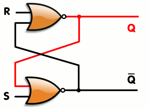
Принцип действия RS-триггера
Память (ОЗУ)
ОЗУ (оперативное запоминающее устройство, англ. RAM) — это большая группа этих самых регистров, соединённых вместе. Память у такого хранилища непостоянная и данные оттуда пропадают при отключении питания. ОЗУ принимает адрес ячейки памяти, в которую нужно поместить данные, сами данные и флаг записи/чтения, который приводит в действие триггеры.
Прим. перев. Оперативная память бывает статической и динамической — SRAM и DRAM соответственно. В статической памяти ячейками являются триггеры, а в динамической — конденсаторы. SRAM быстрее, а DRAM дешевле.
Команды (инструкции)
Команды — это фактические действия, которые компьютер должен выполнять. Они бывают нескольких типов:
- Арифметические: сложение, вычитание, умножение и т. д.
- Логические: И (логическое умножение/конъюнкция), ИЛИ (логическое суммирование/дизъюнкция), отрицание и т. д.
- Информационные:
move,input,outptut,loadиstore. - Команды перехода:
goto,if ... goto,callиreturn. - Команда останова:
halt.
Прим. перев. На самом деле все арифметические операции в АЛУ могут быть созданы на основе всего двух: сложение и сдвиг. Однако чем больше базовых операций поддерживает АЛУ, тем оно быстрее.
Инструкции предоставляются компьютеру на языке ассемблера или генерируются компилятором высокоуровневых языков.
В процессоре инструкции реализуются на аппаратном уровне. За один такт одноядерный процессор может выполнить одну элементарную (базовую) инструкцию.
Группу инструкций принято называть набором команд (англ. instruction set).
Тактирование процессора
Быстродействие компьютера определяется тактовой частотой его процессора. Тактовая частота — количество тактов (соответственно и исполняемых команд) за секунду.
Частота нынешних процессоров измеряется в ГГц (Гигагерцы). 1 ГГц = 10⁹ Гц — миллиард операций в секунду.
Чтобы уменьшить время выполнения программы, нужно либо оптимизировать (уменьшить) её, либо увеличить тактовую частоту. У части процессоров есть возможность увеличить частоту (разогнать процессор), однако такие действия физически влияют на процессор и нередко вызывают перегрев и выход из строя.
Выполнение инструкций
Инструкции хранятся в ОЗУ в последовательном порядке. Для гипотетического процессора инструкция состоит из кода операции и адреса памяти/регистра. Внутри управляющего устройства есть два регистра инструкций, в которые загружается код команды и адрес текущей исполняемой команды. Ещё в процессоре есть дополнительные регистры, которые хранят в себе последние 4 бита выполненных инструкций.
Ниже рассмотрен пример набора команд, который суммирует два числа:
LOAD_A 8. Это команда сохраняет в ОЗУ данные, скажем,<1100 1000>. Первые 4 бита — код операции. Именно он определяет инструкцию. Эти данные помещаются в регистры инструкций УУ. Команда декодируется в инструкциюload_A— поместить данные1000(последние 4 бита команды) в регистрA.LOAD_B 2. Ситуация, аналогичная прошлой. Здесь помещается число 2 (0010) в регистрB.ADD B A. Команда суммирует два числа (точнее прибавляет значение регистраBв регистрA). УУ сообщает АЛУ, что нужно выполнить операцию суммирования и поместить результат обратно в регистрA.STORE_A 23. Сохраняем значение регистраAв ячейку памяти с адресом23.
Вот такие операции нужны, чтобы сложить два числа.
Шина
Все данные между процессором, регистрами, памятью и I/O-устройствами (устройствами ввода-вывода) передаются по шинам. Чтобы загрузить в память только что обработанные данные, процессор помещает адрес в шину адреса и данные в шину данных. Потом нужно дать разрешение на запись на шине управления.
Кэш
У процессора есть механизм сохранения инструкций в кэш. Как мы выяснили ранее, за секунду процессор может выполнить миллиарды инструкций. Поэтому если бы каждая инструкция хранилась в ОЗУ, то её изъятие оттуда занимало бы больше времени, чем её обработка. Поэтому для ускорения работы процессор хранит часть инструкций и данных в кэше.
Если данные в кэше и памяти не совпадают, то они помечаются грязными битами (англ. dirty bit).
Поток инструкций
Современные процессоры могут параллельно обрабатывать несколько команд. Пока одна инструкция находится в стадии декодирования, процессор может успеть получить другую инструкцию.
Однако такое решение подходит только для тех инструкций, которые не зависят друг от друга.
Если процессор многоядерный, это означает, что фактически в нём находятся несколько отдельных процессоров с некоторыми общими ресурсами, например кэшем.
Если хотите узнать о процессорах больше, посмотрите, какие бывают популярные архитектуры: CISC, RISC, MISC и другие и виды.
180К открытий197К показов
Путешествие через вычислительный конвейер процессора
Время на прочтение16 мин
Количество просмотров137K
Так как карьера программиста тесно связана с процессором, неплохо бы знать как он работает.
Что происходит внутри процессора? Сколько времени уходит на исполнение одной инструкции? Что значит, когда новый процессор имеет 12, или 18, или даже 31-уровневый конвейер?
Программы обычно работают с процессором, как с чёрным ящиком. Инструкции входят и выходят из него по порядку, а внутри совершается некая вычислительная магия.
Программисту полезно знать, что происходит внутри этого ящика, особенно, если он будет заниматься оптимизацией программ. Если вы не знаете какие процессы протекают внутри процессора, как вы сможете оптимизировать под него?
Эта статья рассказывает, как устроен вычислительный конвейер x86 процессора.
Вещи, которые вы уже должны знать
Во-первых, предполагается, что вы немного разбираетесь в программировании или может даже немного знаете ассемблер. Если вы не понимаете, что я имею ввиду, когда использую термин «указатель на инструкцию» (instruction pointer), тогда, возможно, эта статья не для вас. Когда я пишу о регистрах, инструкциях и кэшах, я предполагаю, что вы уже знаете, что это значит, можете понять или нагуглить.
Во-вторых, эта статья – упрощение сложной темы. Если вам кажется, что я пропустил какие-то важные моменты, добро пожаловать в комментарии.
В-третьих, я акцентирую внимание только на процессорах Intel x86 семейства. Я знаю о существовании других семейств процессоров, кроме x86. Я знаю, что AMD внесло много полезных нововведений в x86 семейство, и Intel их приняло. Но архитектура и набор инструкций принадлежит Intel, также Intel представило реализацию самых главных особенностей семейства, так что для простоты и логичности, речь пойдет именно об их процессорах.
В-четвертых, эта статья уже устарела. В разработке более новые процессоры, и некоторые из них уже скоро ожидаются в продаже. Я очень рад, что технологии развиваются такими быстрыми темпами и надеюсь, что когда-нибудь все стадии, описанные ниже, полностью устареют и будут заменены еще более удивительными достижениями в процессоростроении.
Основы вычислительного конвейера
Если посмотреть на x86 семейство в целом, то можно заметить, что оно не сильно изменилось за 35 лет. Было много дополнений, но оригинальный дизайн, как и почти весь набор команд, в основном остались нетронутыми и до сих пор прослеживаются в современных процессорах.
Первоначальный 8086 процессор имеет 14 регистров, которые используются до сих пор. Четыре регистра общего назначения – AX, BX, CX и DX. Четыре сегментных регистра, которые используют для облегчения работы с указателями – CS (Code Segment), DS (Data Segment), ES (Extra Segment) и SS (Stack Segment). Четыре индексных регистра, которые указывают на различные адреса в памяти – SI (Source Index), DI (Destination Index), BP (Base Pointer) и SP (Stack Pointer). Один регистр содержит битовые флаги. И, наконец, самый главный регистр в этой статье – IP (Instruction Pointer).
IP регистр – это указатель с особой функцией, его задача указывать на следующую инструкцию, которая подлежит исполнению.
Все процессоры в x86 семействе следуют одному и тому же принципу. Сначала они следуют указателю на инструкцию и декодируют следующую команду по этому адресу. После декодирования следует этап выполнения этой инструкции. Некоторые инструкции читают из памяти или пишут в нее, другие производят вычисления, сравнения или другую работу. Когда работа окончена, команда проходит через этап отставки (retire stage) и IP начинает указывать на следующую инструкцию.
Этот принцип декодирования, выполнения и отставки одинаково применяется как в первом 8086 процессоре, так и в самом последнем Core i7. С течением времени были добавлены новые этапы конвейера, но принцип работы остался прежним.
Что изменилось за 35 лет
Первые процессоры были просты по сегодняшним меркам. 8086 процессор начинал с проверки команды на текущем указателе на инструкцию, декодировал ее, выполнял, отставлял и продолжал работу со следующей инструкцией на которую указывал IP.
Каждый новый чип в семействе добавлял новую функциональность. Большинство добавляло новые инструкции, некоторые добавляли новые регистры. Чтобы оставаться в рамках этой статьи, я буду уделять внимание изменениям, которые непосредственно касаются прохождения команд через ЦП. Другие изменения, такие как добавление виртуальной памяти или параллельной обработки, конечно же интересны, но выходят за рамки данной статьи.
В 1982 был введён кэш инструкций. Вместо обращения к памяти на каждой команде, процессор читал на несколько байт дальше текущего IP. Кэш инструкций был всего несколько байт в размере, достаточным для хранения лишь нескольких команд, но ощутимо увеличивал производительность, исключая постоянные обращения к памяти каждые несколько тактов.
В 1985 в 386 процессор был добавлен кэш данных и увеличен размер кэша инструкций. Этот шаг позволил увеличить производительность за счет чтения на несколько байт дальше запроса на данные. На тот момент кэши данных и инструкций измерялись в килобайтах, нежели в байтах.
В 1989 i486 процессор перешел на 5-уровневый конвейер. Вместо наличия одной инструкции во всем процессоре, теперь каждый уровень конвейера мог иметь по инструкции. Это нововведение позволило увеличить производительность более чем в два раза по сравнению с 386 процессором на той частоте. Этап загрузки (fetch stage) извлекал команду из кэша инструкций (размер кэша в то время был обычно 8кб). Второй этап декодировал инструкцию. Третий этап транслировал адреса памяти и смещения, необходимые для команды. Четвёртый этап выполнял инструкцию. Пятый этап отправлял команду в отставку и записывал результаты обратно в регистры и память по мере необходимости. Появление возможности держать в процессоре множество инструкций одновременно позволило программам выполняться гораздо быстрее.
1993 год был годом появления процессора Pentium. Название семейства процессоров сменилось с номеров на имена из-за судебного процесса, поэтому оно было названо Pentium вместо 586. Конвейер чипа изменился еще больше по сравнению с i486. Архитектура Pentium добавила второй отдельный суперскалярный конвейер. Основной конвейер работал также, как и на i486, в то время как второй выполнял более простые инструкции, такие как целочисленная арифметика, параллельно и намного быстрее.
В 1995 Intel выпустило процессор Pentium Pro, который имел кардинальные изменения в дизайне. У чипа появилось несколько особенностей, включая ядро с внеочерёдным (Out-of-Order, OOO) и упреждающим (Speculative) исполнением команд. Конвейер был расширен до 12 этапов, и в него вошло нечто, называемое суперконвейером (superpipeline), где большое количество инструкций могло исполняться одновременно. OOO ядро будет более подробно освещено ниже в статье.
Между 1995 годом, когда OOO ядро было представлено, и 2002 было сделано много важных изменений. Были добавлены дополнительные регистры и представлены инструкции, которые могли обрабатывать множество данных за раз (Single Instruction Multiple Data, SIMD). Появились новые кэши, старые увеличились в размере. Этапы конвейера делились и объединялись, адаптируясь к требованиям реального мира. Эти и многие другие изменения были важны для общей производительности, но мало что значили, когда речь шла о потоке данных через процессор.
В 2002 Pentium 4 представил новую технологию — Hyper-Threading. OOO ядро было настолько успешным в обработке команд, что способно было обрабатывать инструкции быстрее, чем они могли быть посланы ядру. Для большинства пользователей OOO ядро процессора практически бездействовало большую часть времени даже под нагрузкой. Для обеспечения постоянного потока инструкций к OOO ядру добавили второй фронт-энд. Операционная система видела два процессора вместо одного. Процессор содержал два набора x86 регистров, два декодера инструкций, которые следили за двумя наборами IP и обрабатывали два набора инструкций. Далее команды обрабатывались одним общим OOO ядром, но это было незаметно для программ. Потом инструкции проходили этап отставки, как и ранее, и посылались назад к виртуальным процессорам, на которые они поступали.
В 2006 Intel выпустило микроархитектуру Core. В маркетинговых целях она была названа Core 2 (потому что каждый знает, что два лучше, чем один). Неожиданным ходом было снижение частоты процессоров и отказ от Hyper-Threading. Снижение частот способствовало расширению всех этапов вычислительного конвейера. OOO ядро было расширено, кэши и буферы были увеличены. Архитектура процессоров была переработана с уклоном на двух- и четырёхъядерные чипы с общими кэшами.
В 2008 Intel ввело схему именования процессоров Core i3, Core i5 и Core i7. В этих процессорах вновь появился Hyper-Threading с общим OOO ядром, и отличались они, в основном, лишь размерами кэшей.
Будущие процессоры: Следующее обновление микроархитектуры, названной Haswell, по слухам, будет выпущено во второй половине 2013. Опубликованные на данный момент документы говорят о том, что это будет 14-уровневый конвейер, и, скорей всего, принцип обработки информации будет все также следовать дизайну Pentium Pro.
Так что же такое этот вычислительный конвейер, что такое OOO ядро и как это все увеличивает скорость обработки?
Вычислительный конвейер процессора
В самом простой форме, описанной выше, одиночная инструкция входит в процессор, обрабатывается и выходит с другой стороны. Это довольно интуитивно для большинства программистов.
Процессор i486 имел 5-уровневый конвейер – загрузка (Fetch), основное декодирование (D1), вторичное декодирование или трансляция (D2), выполнение (EX), запись результата в регистры и память (WB). Каждый этап конвейера мог содержать по инструкции.
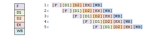
Конвейер i486 и пять инструкций, проходящие через него одновременно.
Однако такая схема имела серьезный недостаток. Представьте себе код ниже. До прихода конвейера следующие три строки кода были распространенным способом поменять значения двух переменных без использования третьей.
XOR a, b
XOR b, a
XOR a, b
Чипы, начиная с 8086 и до 386 не имели внутреннего конвейера. Они обрабатывали только одну инструкцию в каждый момент времени, независимо и полностью. Три последовательных XOR инструкции в такой архитектуре вовсе не проблема.
Теперь подумаем, что происходит с i486, так как это был первый x86 чип с конвейером. Наблюдать за многими вещами в движении одновременно может быть затруднительно, поэтому, возможно, вы сочтёте полезным обратиться к диаграмме выше.
Первая инструкция входит в этап загрузки, на этом первый шаг закончен. Следующий шаг – первая инструкция входит в D1 этап, вторая инструкция помещается в этап загрузки. Третий шаг – первая инструкция двигается в D2 этап, вторая в D1 и третья загружается в Fetch. На следующем шагу что-то идет не так – первая инструкция переходит в EX…, но остальные остаются на месте. Декодер останавливается, потому что вторая XOR команда требует результат первой. Переменная «a» должна быть использована во второй инструкции, но в неё не будет произведена запись, пока не выполнилась первая инструкция. Поэтому команды в конвейере ждут, пока первая команда не пройдет EX и WB этапы. Только после этого вторая инструкция может продолжить свой путь по конвейеру. Третья команда аналогично застрянет в ожидании выполнения второй команды.
Такое явление называется ступор конвейера (pipeline stall) или конвейерный пузырь (pipeline bubble).
Другой проблемой конвейеров является возможность одних инструкций выполняться очень быстро, а других очень медленно, что было более заметно с двойным конвейером Pentium.
Pentium Pro представил с собой 12-уровневый конвейер. Когда это число было впервые озвучено, то понимавшие как работал суперскалярный конвейер программисты затаили дыхание. Если бы Intel последовало такому же принципу с 12-уровневым конвейером, то любой ступор конвейера или медленная инструкция серьезно бы сказывались на производительности. Но в то же время Intel анонсировало кардинально отличающийся конвейер, названный ядром с внеочерёдным исполнением (OOO core). Несмотря на то, что это трудно было понять из документации, Intel заверило разработчиков, что они будут потрясены результатами.
Давайте разберем OOO ядро более детально.
OOO конвейер
В случае с OOO ядром, иллюстрация стоит тысячи слов. Так что давайте посмотрим несколько картинок.
Диаграмы конвейеров процессора
5-уровневый конвейер i486 работал замечательно. Эта идея была довольно распространена среди других семейств процессоров в то время и работала отлично в реальных условиях.
Суперскалярный конвейер i486.
Конвейер Pentium был даже еще лучше i486. Он имел два вычислительных конвейера, которые могли работать параллельно, и каждый из них мог содержать множество инструкций на различных этапах, позволяя вам обрабатывать почти в двое больше инструкций за то же время.
Два параллельных суперскалярных конвейера Pentium.
Однако наличие быстрых команд, ожидающих выполнение медленных, было все также проблемой в параллельных конвейерах, как и наличие последовательных команд (привет ступор). Конвейеры были все так же линейными и могли сталкиваться с непреодолимыми ограничениями производительности.
Дизайн OOO ядра сильно отличался от предыдущих чипов с линейными путями. Сложность конвейера возросла, и были введены нелинейные пути.
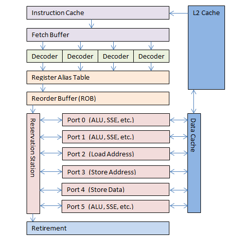
OOO ядро, используемое с 1995 года. Цветовое обозначение соответствует пяти этапам, используемых в предыдущих процессорах. Некоторые этапы и буферы не показаны, так как варьируются от процессора к процессору.
Сначала инструкции загружаются из памяти и помещаются в кэш инструкций процессора. Декодер современного процессора может предсказать появление скорого ветвления (например вызов функции) и начать загрузку инструкций заранее.
Этап декодирования был немного изменен по сравнению с более ранними чипами. Вместо обработки лишь одной инструкции на IP, Pentium Pro мог декодировать до трех инструкций за такт. Сегодняшние процессоры (2008-2013) могут декодировать до четырёх инструкций за такт. Результатом декодирования являются микрооперации (micro-ops / µ-ops).
Следующий этап (или группа этапов) состоит из трансляции микроопераций (micro-op transaltion) и последующего присвоения псевдонимов регистрам (register aliasing). Множество операций выполняются одновременно, возможно внеочерёдно, поэтому одна инструкция может читать из регистра, пока другая в него пишет. Запись в регистр может подавить значение, нужное другой инструкции. Оригинальные регистры внутри процессора (AX, BX, CX, DX итд.) транслируются (или создаются псевдонимы) во внутренние, скрытые от программиста регистры. Значение регистров и адресов памяти затем должны быть привязаны к временным значениям для обработки. На данный момент 4 микрооперации могут проходить через этап трансляции за такт.
После трансляции все микрооперации входят в буфер переупорядочивания (reorder buffer, ROB). На данный момент этот буфер может вмещать до 128 микроопераций. На процессорах с HT ROB также может выступать в роли координатора входных команд с виртуальных процессоров, распределяя два потока команд на одно OOO ядро.
Теперь микрооперации готовы для обработки и помещаются в резервацию (reservation station, RS). RS на данный момент может вмещать 36 микроопераций в любой момент времени.
Теперь настало время для магии OOO ядра. Микрооперации обрабатываются одновременно на множестве исполнительных блоков (execution unit), причем каждый блок работает максимально быстро. Микрооперации могут обрабатываться внеочерёдно, если все нужные данные для этого уже доступны. Если данные недоступны, выполнение откладывается до их готовности, пока выполняются другие готовые микрооперации. Таким образом долгие операции не блокируют быстрые и последствия ступора конвейера уже не так печальны.
OOO ядро Pentium Pro имело шесть исполнительных блоков: два для работы с целыми числами, один для чисел с плавающей точкой, загрузочный блок, блок сохранения адресов и блок сохранения данных. Два целочисленных блока были специализированы, один мог работать со сложными операциями, другой мог обрабатывать две простые операции за раз. В идеальных условиях исполнительные блоки Pentium Pro могли обрабатывать семь микроопераций за такт.
Сегодняшнее OOO ядро также содержит шесть исполнительных блоков. Оно до сих пор содержит блоки загрузки адреса, сохранения адреса и сохранения данных. Однако остальные три немного изменились. Каждый из трех блоков теперь может выполнять простые математические операции или более сложную микрооперацию. Каждый из трех блоков специализирован для конкретных микроопераций, позволяя выполнять работу быстрее, по сравнению с блоками общего назначения. В идеальных условиях нынешнее OOO ядро может обрабатывать 11 микроопераций за такт.
Наконец микрооперация начинает выполняться. Она проходит через более мелкие этапы (отличающиеся между процессорами) и проходит этап отставки. В этот момент микрооперация возвращается во внешний мир и IP начинает указывать на следующую инструкцию. С точки зрения программы, инструкция просто входит в процессор и выходит с другой стороны, точно так же, как это было со старым 8086.
Если вы внимательно читали статью, вы возможно могли заметить очень важную проблему в описании выше. Что произойдет в случае смены места исполнения? Например, что произойдет, если код доходит до if или switch конструкции? В более старых процессорах это значило сброс всей работы в суперскалярном конвейере и ожидание начала обработки новой ветки исполнения.
Ступор конвейера, когда в процессоре находится сотня или более инструкций очень серьезно сказывается на производительности. Каждая инструкция вынуждена ждать, пока инструкции с нового адреса будут загружены и конвейер будет перезапущен. В этой ситуации OOO ядро должно отменить всю текущую работу, откатиться до предыдущего состояния, подождать, пока все микрооперации пройдут отставку, отбросить их вместе с результатами и затем продолжить работу по новому адресу. Эта проблема была очень серьёзной и часто случалась при проектировании. Показатели производительности в такой ситуации были неприемлемы для инженеров. Именно здесь приходит на помощь еще одна важная особенность OOO ядра.
Их ответ был – упреждающее выполнение. Упреждающее выполнение означает, что когда OOO ядро встречает в коде условные конструкции (например if блок), оно просто загрузит и выполнит две ветки кода. Как только ядро понимает, какая ветка верная, результаты второй будут сброшены. Это предотвращает ступор конвейера ценой незначительных издержек на запуск кода в неверной ветке. Также был добавлен кэш для предсказания ветвления (branch prediction cache), который намного улучшил результаты в ситуациях, когда ядро было вынуждено прогнозировать среди множества условных переходов. Ступоры конвейера до сих пор встречаются из-за ветвления, однако это решение позволило сделать их редким исключением, нежели обычным явлением.
Ну и наконец, процессор с HT предоставляет два виртуальных процессора для одного общего OOO ядра. Они разделяют общий ROB и OOO ядро и будут видны для операционной системы как два отдельных процессора. Это выглядит примерно так:
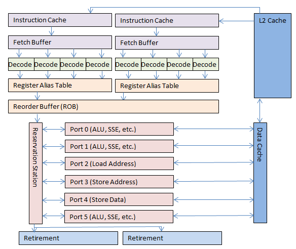
OOO ядро с Hyper-Threading, см. примечание.
Процессор с HT получает два виртуальных процессора, которые взамен поставляют больше данных OOO ядру, что дает увеличение производительности при обычном пользовании. Лишь некоторые тяжелые вычислительные нагрузки, оптимизированные под многопроцессорные системы, могут полностью загрузить OOO ядро. В этом случае HT может несколько понизить производительность. Однако такие нагрузки относительно редки. Для потребителя HT обычно позволяет увеличивать скорость работы примерно вдвое при обычном ежедневном пользовании компьютером.
Пример
Всё это может показаться немного запутанным. Надеюсь, пример расставит всё на свои места.
С точки зрения приложения, мы все ещё работаем на вычислительном конвейере старого 8086. Это чёрный ящик. Инструкция, на которую указывает IP, обрабатывается этим ящиком, и, когда инструкция выходит из него, результаты уже отображены в памяти.
Хотя с точки зрения инструкции, этот чёрный ящик то ещё приключение.
Ниже приводится путь, который совершает инструкция в современном процессоре (2008-2013).
Поехали, вы – инструкция в программе, и эта программа запускается.
Вы терпеливо ждете, пока IP начнет указывать на вас для последующей обработки. Когда IP указывает примерно за 4кб до вашего расположения, или за 1500 инструкций, вы перемещаетесь в кэш инструкций. Загрузка в кэш занимает некоторое время, но это не страшно, так как вы ещё нескоро будете запущены. Эта предзагрузка (prefetch) является частью первого этапа конвейера.
Тем временем IP указывает всё ближе и ближе к вам, и, когда он начинает указывать за 24 инструкции до вас, вы и пять соседних команд отправляетесь в очередь инструкций (instruction queue).
Этот процессор имеет четыре декодера, которые могут вмещать одну сложную команду и до трёх простых. Так случилось, что вы сложная инструкция и были декодированы в четыре микрооперации.
Декодирование – это многоуровневый процесс. Часть декодирования включает в себя анализ на предмет требуемых вами данных и вероятность перехода в какое-то новое место. Декодер зафиксировал потребность в дополнительных данных. Без вашего участия, где-то на другом конце компьютера, нужные вам данные начинают загрузку в кэш данных.
Ваши четыре микрооперации подходят к таблице псевдонимов регистров. Вы объявляете с какого адреса памяти вы читаете (это оказывается fs:[eax+18h]), и чип транслирует его во временный адрес для ваших микроопераций. Ваши микрооперации входят в ROB, откуда, при первой же возможности, двигаются в резервацию.
Резервация содержит инструкции, готовые к исполнению. Ваша третья микрооперация немедленно подхватывается пятым портом исполнения. Вам не известно, почему она была выбрана первой, но её уже нет. Через несколько тактов ваша первая микрооперация устремляется во второй порт, блок загрузки адресов. Оставшиеся микрооперации ждут, пока различные порты подхватывают другие микрооперации. Они ждут, пока второй порт загружает данные из кэша данных во временные слоты памяти.
Долго ждут…
Очень долго ждут…
Другие инструкции приходят и уходят, в то время как ваши микрооперации ждут своего друга, пока тот загружает нужные данные. Хорошо, что этот процессор знает как обрабатывать их внеочерёдно.
Внезапно, обе оставшиеся микрооперации подхватываются нулевым и первым портом, должно быть загрузка данных завершена. Все микрооперации запущены и со временем они вновь встречаются в резервации.
По пути обратно через ворота, микрооперации передают свои билеты с временными адресами. Микрооперации собираются и объединяются, и вы вновь, как инструкция, чувствуете себя единым целым. Процессор вручает вам ваш результат и вежливо направляет к выходу.
Через дверь с пометкой “Отставка” стоит короткая очередь. вы встаете в очередь и обнаруживаете, что вы стоите за той же инструкцией, за которой и заходили. Вы даже стоите в том же порядке. Получается, что OOO ядро действительно знает своё дело.
Со стороны выглядит так, что каждая выходящая из процессора команда выходит по одной, точно в таком же порядке, в каком IP указывал на них.
Заключение
Надеюсь, что эта маленькая лекция пролила немного света на то, что происходит внутри процессора. Как видите, здесь нет магии, дыма и зеркал.
Теперь мы можем ответить на вопросы, заданные в начале статьи.
Так что же происходит внутри процессора? Это сложный мир, где инструкции разбиваются на микрооперации, обрабатываются при первой же возможности и в любом порядке, и вновь собираются воедино, сохраняя свой порядок и расположение. Для внешнего мира выглядит так, будто они обрабатываются последовательно и независимо друг от друга. Но мы теперь знаем, что на самом деле, они обрабатываются внеочерёдно, иногда даже предсказывая и запуская вероятные ветки кода.
Сколько времени уходит на исполнение одной инструкции? Тогда как в бесконвейерном мире для этого имелся хороший ответ, в современном же процессоре всё зависит от того какие инструкции находятся рядом, какой размер соседних кэшей и что в них находится. Есть минимальное время прохождения команды через процессор, но эта величина практически постоянна. Хороший программист или оптимизирующий компилятор может заставить множество инструкций исполняться за среднее время близкое к нулю. Среднее время близкое к нулю – это не время исполнения самой медленной инструкции, а время, требуемое для прохождения инструкции через OOO ядро и время, требуемое кэшу для загрузки и выгрузки данных.
Что значит, когда новый процессор имеет 12, или 18, или даже 31-уровневый конвейер? Это значит, что больше инструкций за раз могут быть приглашены на вечеринку. Очень длинный конвейер может значить, что несколько сотен инструкций могут быть помечены как “обрабатываются” за раз. Когда все идет по плану, OOO ядро постоянно загружено и пропускная способность процессора просто впечатляет. К сожалению, это так же значит, что ступор конвейера перерастает из мелкой неприятности, как это было раньше, в кошмар, так как сотни команд будут вынуждены ожидать очистки конвейера.
Как вы можете применить эти знания в своих программах? Хорошие новости – процессор может предугадать большинство распространённых шаблонов кода, и компиляторы оптимизируют код для OOO ядра уже почти два десятилетия. Процессор лучше всего работает с упорядоченными инструкциями и данными. Всегда пишите простой код. Простой и не извилистый код поможет оптимизатору компилятора найти и ускорить результаты. Если возможно, не создавайте переходы по коду. Если вам необходимо совершать переходы, пытайтесь делать это, следуя определенному шаблону. Сложные дизайны, наподобие динамических таблиц переходов, выглядят классно и многое могут, но ни компилятор, ни процессор, не смогут спрогнозировать какой кусок кода будет выполняться в следующий момент времени. Поэтому сложный код с большой вероятностью будет провоцировать ступоры и неверные предсказания ветвления. Напротив, поддерживайте ваши данные простыми. Организуйте данные упорядоченно, связанно и последовательно для предотвращения ступоров. Правильный выбор структуры и разметки данных может заметно сказаться на повышении производительности. До тех пор, пока ваши данные и код остаются простыми, вы обычно можете положиться на работу оптимизирующего компилятора.
Спасибо, что были частью этого путешествия.
Оригинал — www.gamedev.net/page/resources/_/technical/general-programming/a-journey-through-the-cpu-pipeline-r3115
From Wikipedia, the free encyclopedia
The x86 instruction set refers to the set of instructions that x86-compatible microprocessors support. The instructions are usually part of an executable program, often stored as a computer file and executed on the processor.
The x86 instruction set has been extended several times, introducing wider registers and datatypes as well as new functionality.[1]
x86 integer instructions
[edit]
Below is the full 8086/8088 instruction set of Intel (81 instructions total).[2] These instructions are also available in 32-bit mode, in which they operate on 32-bit registers (eax, ebx, etc.) and values instead of their 16-bit (ax, bx, etc.) counterparts. The updated instruction set is grouped according to architecture (i186, i286, i386, i486, i586/i686) and is referred to as (32-bit) x86 and (64-bit) x86-64 (also known as AMD64).
Original 8086/8088 instructions
[edit]
This is the original instruction set. In the ‘Notes’ column, r means register, m means memory address and imm means immediate (i.e. a value).
Added in specific processors
[edit]
The new instructions added in 80286 add support for x86 protected mode. Some but not all of the instructions are available in real mode as well.
- ^ a b c d The descriptors used by the
LGDT,LIDT,SGDTandSIDTinstructions consist of a 2-part data structure. The first part is a 16-bit value, specifying table size in bytes minus 1. The second part is a 32-bit value (64-bit value in 64-bit mode), specifying the linear start address of the table.
ForLGDTandLIDTwith a 16-bit operand size, the address is ANDed with 00FFFFFFh.On Intel (but not AMD) CPUs, the
SGDTandSIDTinstructions with a 16-bit operand size is – as of Intel SDM revision 079 – documented to write a descriptor to memory with the last byte being set to 0. However, observed behavior is that bits 31:24 of the descriptor table address are written instead.[4] - ^ a b c d The
LGDT,LIDT,LLDTandLTRinstructions are serializing on Pentium and later processors. - ^ The
LMSWinstruction is serializing on Intel processors from Pentium onwards, but not on AMD processors. - ^ On 80386 and later, the «Machine Status Word» is the same as the CR0 control register – however, the
LMSWinstruction can only modify the bottom 4 bits of this register and cannot clear bit 0. The inability to clear bit 0 means thatLMSWcan be used to enter but not leave x86 Protected Mode.
On 80286, it is not possible to leave Protected Mode at all (neither withLMSWnor withLOADALL[5]) without a CPU reset – on 80386 and later, it is possible to leave Protected Mode, but this requires the use of the 80386-and-laterMOVtoCR0instruction. - ^ If
CR4.UMIP=1is set, then theSGDT,SIDT,SLDT,SMSWandSTRinstructions can only run in Ring 0.
These instructions were unprivileged on all x86 CPUs from 80286 onwards until the introduction of UMIP in 2017.[6]
This has been a significant security problem for software-based virtualization, since it enables these instructions to be used by a VM guest to detect that it is running inside a VM.[7] - ^ a b c The
SMSW,SLDTandSTRinstructions always use an operand size of 16 bits when used with a memory argument. With a register argument on 80386 or later processors, wider destination operand sizes are available and behave as follows:SMSW: Stores full CR0 in x86-64 long mode, undefined otherwise.SLDT: Zero-extends 16-bit argument on Pentium Pro and later processors, undefined on earlier processors.STR: Zero-extends 16-bit argument.
- ^ In 64-bit long mode, the
ARPLinstruction is not available – the63 /ropcode has been reassigned to the 64-bit-mode-onlyMOVSXDinstruction. - ^ The
ARPLinstruction causes #UD in Real mode and Virtual 8086 Mode – Windows 95 and OS/2 2.x are known to make extensive use of this #UD to use the63opcode as a one-byte breakpoint to transition from Virtual 8086 Mode to kernel mode.[8][9] - ^ Bits 19:16 of this mask are documented as «undefined» on Intel CPUs.[10] On AMD CPUs, the mask is documented as
0x00FFFF00. - ^ a b For the
LARandLSLinstructions, if the specified segment descriptor could not be loaded, then the instruction’s destination register is left unmodified. - ^ On some Intel CPU/microcode combinations from 2019 onwards, the
VERWinstruction also flushes microarchitectural data buffers. This enables it to be used as part of workarounds for Microarchitectural Data Sampling security vulnerabilities.[11][12] Some of the microarchitectural buffer-flushing functions that have been added toVERWmay require the instruction to be executed with a memory operand.[13] - ^ a b Undocumented, 80286 only.[5][14][15] (A different variant of
LOADALLwith a different opcode and memory layout exists on 80386.)
The 80386 added support for 32-bit operation to the x86 instruction set. This was done by widening the general-purpose registers to 32 bits and introducing the concepts of OperandSize and AddressSize – most instruction forms that would previously take 16-bit data arguments were given the ability to take 32-bit arguments by setting their OperandSize to 32 bits, and instructions that could take 16-bit address arguments were given the ability to take 32-bit address arguments by setting their AddressSize to 32 bits. (Instruction forms that work on 8-bit data continue to be 8-bit regardless of OperandSize. Using a data size of 16 bits will cause only the bottom 16 bits of the 32-bit general-purpose registers to be modified – the top 16 bits are left unchanged.)
The default OperandSize and AddressSize to use for each instruction is given by the D bit of the segment descriptor of the current code segment — D=0 makes both 16-bit, D=1 makes both 32-bit. Additionally, they can be overridden on a per-instruction basis with two new instruction prefixes that were introduced in the 80386:
66h: OperandSize override. Will change OperandSize from 16-bit to 32-bit ifCS.D=0, or from 32-bit to 16-bit ifCS.D=1.67h: AddressSize override. Will change AddressSize from 16-bit to 32-bit ifCS.D=0, or from 32-bit to 16-bit ifCS.D=1.
The 80386 also introduced the two new segment registers FS and GS as well as the x86 control, debug and test registers.
The new instructions introduced in the 80386 can broadly be subdivided into two classes:
- Pre-existing opcodes that needed new mnemonics for their 32-bit OperandSize variants (e.g.
CWDE,LODSD) - New opcodes that introduced new functionality (e.g.
SHLD,SETcc)
For instruction forms where the operand size can be inferred from the instruction’s arguments (e.g. ADD EAX,EBX can be inferred to have a 32-bit OperandSize due to its use of EAX as an argument), new instruction mnemonics are not needed and not provided.
- ^ For the 32-bit string instructions, the ±± notation is used to indicate that the indicated register is post-decremented by 4 if
EFLAGS.DF=1and post-incremented by 4 otherwise.
For the operands where the DS segment is indicated, the DS segment can be overridden by a segment-override prefix – where the ES segment is indicated, the segment is always ES and cannot be overridden.
The choice of whether to use the 16-bit SI/DI registers or the 32-bit ESI/EDI registers as the address registers to use is made by AddressSize, overridable with the67prefix. - ^ The 32-bit string instructions accept repeat-prefixes in the same way as older 8/16-bit string instructions.
ForLODSD,STOSD,MOVSD,INSDandOUTSD, theREPprefix (F3) will repeat the instruction the number of times specified in rCX (CX or ECX, decided by AddressSize), decrementing rCX for each iteration (with rCX=0 resulting in no-op and proceeding to the next instruction).
ForCMPSDandSCASD, theREPE(F3) andREPNE(F2) prefixes are available, which will repeat the instruction, decrementing rCX for each iteration, but only as long as the flag condition (ZF=1 forREPE, ZF=0 forREPNE) holds true AND rCX ≠ 0. - ^ For the
INSB/W/Dinstructions, the memory access rights for theES:[rDI]memory address might not be checked until after the port access has been performed – if this check fails (e.g. page fault or other memory exception), then the data item read from the port is lost. As such, it is not recommended to use this instruction to access an I/O port that performs any kind of side effect upon read. - ^ I/O port access is only allowed when CPL≤IOPL or the I/O port permission bitmap bits for the port to access are all set to 0.
- ^ The
CWDEinstruction differs from the olderCWDinstruction in thatCWDwould sign-extend the 16-bit value in AX into a 32-bit value in the DX:AX register pair. - ^ For the
E3opcode (JCXZ/JECXZ), the choice of whether the instruction will useCXorECXfor its comparison (and consequently which mnemonic to use) is based on the AddressSize, not OperandSize. (OperandSize instead controls whether the jump destination should be truncated to 16 bits or not).
This also applies to the loop instructionsLOOP,LOOPE,LOOPNE(opcodesE0,E1,E2), however, unlikeJCXZ/JECXZ, these instructions have not been given new mnemonics for their ECX-using variants. - ^ For
PUSHA(D), the value of SP/ESP pushed onto the stack is the value it had just before thePUSHA(D)instruction started executing. - ^ For
POPA/POPAD, the stack item corresponding to SP/ESP is popped off the stack (performing a memory read), but not placed into SP/ESP. - ^ The
PUSHFDandPOPFDinstructions will cause a #GP exception if executed in virtual 8086 mode if IOPL is not 3.
ThePUSHF,POPF,IRETandIRETDinstructions will cause a #GP exception if executed in Virtual-8086 mode if IOPL is not 3 and VME is not enabled. - ^ If
IRETDis used to return from kernel mode to user mode (which will entail a CPL change) and the user-mode stack segment indicated by SS is a 16-bit segment, then theIRETDinstruction will only restore the low 16 bits of the stack pointer (ESP/RSP), with the remaining bits keeping whatever value they had in kernel code before theIRETD. This has necessitated complex workarounds on both Linux («ESPFIX»)[16] and Windows.[17] This issue also affects the later 64-bitIRETQinstruction.
- ^ a b c d For the
BT,BTS,BTRandBTCinstructions:- If the first argument to the instruction is a register operand and/or the second argument is an immediate, then the bit-index in the second argument is taken modulo operand size (16/32/64, in effect using only the bottom 4, 5 or 6 bits of the index.)
- If the first argument is a memory operand and the second argument is a register operand, then the bit-index in the second argument is used in full – it is interpreted as a signed bit-index that is used to offset the memory address to use for the bit test.
- ^ a b c The
BTS,BTCandBTRinstructions accept theLOCK(F0) prefix when used with a memory argument – this results in the instruction executing atomically. - ^ If the
F3prefix is used with the0F BC /ropcode, then the instruction will execute asTZCNTon systems that support the BMI1 extension.TZCNTdiffers fromBSFin thatTZCNTbut notBSRis defined to return operand size if the source operand is zero – for other source operand values, they produce the same result (except for flags). - ^ a b
BSFandBSRset the EFLAGS.ZF flag to 1 if the source argument was all-0s and 0 otherwise.
If the source argument was all-0s, then the destination register is documented as being left unchanged on AMD processors, but set to an undefined value on Intel processors. - ^ If the
F3prefix is used with the0F BD /ropcode, then the instruction will execute asLZCNTon systems that support the ABM or LZCNT extensions.LZCNTproduces a different result fromBSRfor most input values. - ^ a b For
SHLDandSHRD, the shift-amount is masked – the bottom 5 bits are used for 16/32-bit operand size and 6 bits for 64-bit operand size.SHLDandSHRDwith 16-bit arguments and a shift-amount greater than 16 produce undefined results. (Actual results differ between different Intel CPUs, with at least three different behaviors known.[18]) - ^ a b The condition codes supported for the
SETccandJcc nearinstructions (opcodes0F 9x /0and0F 8xrespectively, with the x nibble specifying the condition) are:
x cc Condition (EFLAGS) 0 O OF=1: «Overflow» 1 NO OF=0: «Not Overflow» 2 C,B,NAE CF=1: «Carry», «Below», «Not Above or Equal» 3 NC,NB,AE CF=0: «Not Carry», «Not Below», «Above or Equal» 4 Z,E ZF=1: «Zero», «Equal» 5 NZ,NE ZF=0: «Not Zero», «Not Equal» 6 NA,BE (CF=1 or ZF=1): «Not Above», «Below or Equal» 7 A,NBE (CF=0 and ZF=0): «Above», «Not Below or Equal» 8 S SF=1: «Sign» 9 NS SF=0: «Not Sign» A P,PE PF=1: «Parity», «Parity Even» B NP,PO PF=0: «Not Parity», «Parity Odd» C L,NGE SF≠OF: «Less», «Not Greater Or Equal» D NL,GE SF=OF: «Not Less», «Greater Or Equal» E LE,NG (ZF=1 or SF≠OF): «Less or Equal», «Not Greater» F NLE,G (ZF=0 and SF=OF): «Not Less or Equal», «Greater» - ^ For
SETcc, while the opcode is commonly specified as /0 – implying that bits 5:3 of the instruction’s ModR/M byte should be 000 – modern x86 processors (Pentium and later) ignore bits 5:3 and will execute the instruction asSETccregardless of the contents of these bits. - ^ For
LFS,LGSandLSS, the size of the offset part of the far pointer is given by operand size – the size of the segment part is always 16 bits. In 64-bit mode, using theREX.Wprefix with these instructions will cause them to load a far pointer with a 64-bit offset on Intel but not AMD processors. - ^ a b c d e f For
MOVto/from theCRx,DRxandTRxregisters, the reg part of the ModR/M byte is used to indicateCRx/DRx/TRxregister and r/m part the general-register.Uniquely for the
MOV CRx/DRx/TRxopcodes, the top two bits of the ModR/M byte is ignored – these opcodes are decoded and executed as if the top two bits of the ModR/M byte are11b. - ^ a b c d For moves to/from the
CRxandDRxregisters, the operand size is always 64 bits in 64-bit mode and 32 bits otherwise. - ^ On processors that support global pages (Pentium and later), global page table entries will not be flushed by a
MOVtoCR3− instead, these entries can be flushed by toggling the CR4.PGE bit.
On processors that support PCIDs, writing to CR3 while PCIDs are enabled will only flush TLB entries belonging to the PCID specified in bits 11:0 of the value written to CR3 (this flush can be suppressed by setting bit 63 of the written value to 1). Flushing pages belonging to other PCIDs can instead be done by toggling the CR4.PGE bit, clearing the CR4.PCIDE bit, or using theINVPCIDinstruction. - ^ On processors prior to Pentium, moves to
CR0would not serialize the instruction stream – in part for this reason, it is usually required to perform a far jump[19] immediately after aMOVtoCR0if such aMOVis used to enable/disable protected mode and/or memory paging.MOVtoCR2is architecturally listed as serializing, but has been reported to be non-serializing on at least some Intel Core-i7 processors.[20]MOVtoCR8(introduced with x86-64) is serializing on AMD but not Intel processors. - ^ a b The
MOV TRxinstructions were discontinued from Pentium onwards. - ^ The
INT1/ICEBP(F1) instruction is present on all known Intel x86 processors from the 80386 onwards,[21] but only fully documented for Intel processors from the May 2018 release of the Intel SDM (rev 067) onwards.[22] Before this release, mention of the instruction in Intel material was sporadic, e.g. AP-526 rev 001.[23]
For AMD processors, the instruction has been documented since 2002.[24] - ^ The operation of the
F1(ICEBP) opcode differs from the operation of the regular software interrupt opcodeCD 01in several ways:- In protected mode,
- In virtual-8086 mode,
CD 01will also check CPL against IOPL as an access-rights check, whileF1will not. - In virtual-8086 mode with VME enabled, interrupt redirection is supported for
CD 01but notF1.
CD 01will check CPL against the interrupt descriptor’s DPL field as an access-rights check, whileF1will not. - In virtual-8086 mode,
- ^ The UMOV instruction is present on 386 and 486 processors only.[21]
- ^ a b The
XBTSandIBTSinstructions were discontinued with the B1 stepping of 80386.
They have been used by software mainly for detection of the buggy[25] B0 stepping of the 80386. Microsoft Windows (v2.01 and later) will attempt to run theXBTSinstruction as part of its CPU detection ifCPUIDis not present, and will refuse to boot ifXBTSis found to be working.[26] - ^ a b For
XBTSandIBTS, the r/m argument represents the data to extract/insert a bitfield from/to, the reg argument the bitfield to be inserted/extracted, AX/EAX a bit-offset and CL a bitfield length.[27] - ^ Undocumented, 80386 only.[28]
| Instruction | Opcode | Description | Ring |
|---|---|---|---|
BSWAP r32
|
0F C8+r
|
Byte Order Swap. Usually used to convert between big-endian and little-endian data representations. For 32-bit registers, the operation performed is:
r =   (r << 24)
    | ((r << 8) & 0x00FF0000)
    | ((r >> 8) & 0x0000FF00)
    | (r >> 24);
Using |
3 |
CMPXCHG r/m8,r8
|
0F B0 /r[b]
|
Compare and Exchange. If accumulator (AL/AX/EAX/RAX) compares equal to first operand,[c] then EFLAGS.ZF is set to 1 and the first operand is overwritten with the second operand. Otherwise, EFLAGS.ZF is set to 0, and first operand is copied into the accumulator.
Instruction atomic only if used with |
|
CMPXCHG r/m,r16CMPXCHG r/m,r32
|
0F B1 /r[b]
|
||
XADD r/m,r8
|
0F C0 /r
|
eXchange and ADD. Exchanges the first operand with the second operand, then stores the sum of the two values into the destination operand.
Instruction atomic only if used with |
|
XADD r/m,r16XADD r/m,r32
|
0F C1 /r
|
||
INVLPG m8
|
0F 01 /7
|
Invalidate the TLB entries that would be used for the 1-byte memory operand.[d]
Instruction is serializing. |
0 |
INVD
|
0F 08
|
Invalidate Internal Caches.[e] Modified data in the cache are not written back to memory, potentially causing data loss.[f] | |
WBINVD
|
NFx 0F 09[g]
|
Write Back and Invalidate Cache.[e] Writes back all modified cache lines in the processor’s internal cache to main memory and invalidates the internal caches. |
- ^ Using
BSWAPwith 16-bit registers is not disallowed per se (it will execute without producing an #UD or other exceptions) but is documented to produce undefined results – it is reported to produce various different results on 486,[29] 586, and Bochs/QEMU.[30] - ^ a b On Intel 80486 stepping A,[31] the
CMPXCHGinstruction uses a different encoding —0F A6 /rfor 8-bit variant,0F A7 /rfor 16/32-bit variant. The0F B0/B1encodings are used on 80486 stepping B and later.[32][33] - ^ The
CMPXCHGinstruction setsEFLAGSin the same way as aCMPinstruction that uses the accumulator (AL/AX/EAX/RAX) as its first argument would do. - ^
INVLPGexecutes as no-operation if the m8 argument is invalid (e.g. unmapped page or non-canonical address).INVLPGcan be used to invalidate TLB entries for individual global pages. - ^ a b The
INVDandWBINVDinstructions will invalidate all cache lines in the CPU’s L1 caches. It is implementation-defined whether they will invalidate L2/L3 caches as well.
These instructions are serializing – on some processors, they may block interrupts until completion as well. - ^ Under Intel VT-x virtualization, the
INVDinstruction will cause a mandatory #VMEXIT. Also, on processors that support Intel SGX, if the PRM (Processor Reserved Memory) has been set up by using the PRMRRs (PRM range registers), then theINVDinstruction is not permitted and will cause a #GP(0) exception.[34] - ^ If the
F3prefix is used with the0F 09opcode, then the instruction will execute asWBNOINVDon processors that support the WBNOINVD extension – this will not invalidate the cache.
Integer/system instructions that were not present in the basic 80486 instruction set, but were added in various x86 processors prior to the introduction of SSE. (Discontinued instructions are not included.)
- ^ a b c In 64-bit mode, the
RDMSR,RDTSCandRDPMCinstructions will set the top 32 bits of RDX and RAX to zero. - ^ On Intel and AMD CPUs, the
WRMSRinstruction is also used to update the CPU microcode. This is done by writing the virtual address of the new microcode to upload to MSR79hon Intel CPUs and MSRC001_0020h[36] on AMD CPUs. - ^ Writes to the following MSRs are not serializing:[37][38]
Number Name 48hSPEC_CTRL 49hPRED_CMD 10BhFLUSH_CMD 122hTSX_CTRL 6E0hTSC_DEADLINE 6E1hPKRS 774hHWP_REQUEST
(non-serializing only if the FAST_IA32_HWP_REQUEST bit it set)802hto83Fh(x2APIC MSRs) 1B01hUARCH_MISC_CTL C001_0100hFS_BASE (non-serializing on AMD Zen 4 and later)[39] C001_0101hGS_BASE (Zen 4 and later) C001_0102hKernelGSbase (Zen 4 and later) C001_011BhDoorbell Register (AMD-specific) WRMSRto the x2APIC ICR (Interrupt Command Register; MSR830h) is commonly used to produce an IPI (Inter-processor interrupt) — on Intel[40] but not AMD[41] CPUs, such an IPI can be reordered before an older memory store. - ^ System Management Mode and the
RSMinstruction were made available on non-SL variants of the Intel 486 only after the initial release of the Intel Pentium in 1993. - ^ On some older 32-bit processors, executing
CPUIDwith a leaf index (EAX) greater than 0 may leave EBX and ECX unmodified, keeping their old values. For this reason, it is recommended to zero out EBX and ECX before executingCPUID.
Processors noted to exhibit this behavior include Cyrix MII[46] and IDT WinChip 2.[47]In 64-bit mode,
CPUIDwill set the top 32 bits of RAX, RBX, RCX and RDX to zero. - ^ On some Intel processors starting from Ivy Bridge, there exists MSRs that can be used to restrict
CPUIDto ring 0. Such MSRs are documented for at least Ivy Bridge[48] and Denverton.[49]
The ability to restrictCPUIDto ring 0 also exists on AMD processors supporting the «CpuidUserDis» feature (Zen 4 «Raphael» and later).[50] - ^ a b
CPUIDis also available on some Intel and AMD 486 processor variants that were released after the initial release of the Intel Pentium. - ^ On the Cyrix 5×86 and 6×86 CPUs,
CPUIDis not enabled by default and must be enabled through a Cyrix configuration register. - ^ On NexGen CPUs,
CPUIDis only supported with some system BIOSes. On some NexGen CPUs that do supportCPUID, EFLAGS.ID is not supported but EFLAGS.AC is, complicating CPU detection.[51] - ^ Unlike the older
CMPXCHGinstruction, theCMPXCHG8Binstruction does not modify any EFLAGS bits other than ZF. - ^
LOCK CMPXCHG8Bwith a register operand (which is an invalid encoding) will, on some Intel Pentium CPUs, cause a hang rather than the expected #UD exception — this is known as the Pentium F00F bug. - ^ a b c On IDT WinChip, Transmeta Crusoe and Rise mP6 processors, the
CMPXCHG8Binstruction is always supported, however its CPUID bit may be missing. This is a workaround for a bug in Windows NT.[52] - ^ a b The
RDTSCandRDPMCinstructions are not ordered with respect to other instructions, and may sample their respective counters before earlier instructions are executed or after later instructions have executed. Invocations ofRDPMC(but notRDTSC) may be reordered relative to each other even for reads of the same counter.
In order to impose ordering with respect to other instructions,LFENCEor serializing instructions (e.g.CPUID) are needed.[53] - ^ Fixed-rate TSC was introduced in two stages:
- Constant TSC
- TSC running at a fixed rate as long as the processor core is not in a deep-sleep (C2 or deeper) mode, but not synchronized between CPU cores. Introduced in Intel Prescott, Yonah and Bonnell. Also present in all Transmeta and VIA Nano[54] CPUs. Does not have a CPUID bit.
- Invariant TSC
- TSC running at a fixed rate, and remaining synchronized between CPU cores in all P-,C- and T-states (but not necessarily S-states).
Present in AMD K10 and later; Intel Nehalem/Saltwell[55] and later; Zhaoxin WuDaoKou[56] and later. Indicated with a CPUID bit (leaf8000_0007:EDX[8]).
- ^
RDTSCcan be run outside Ring 0 only ifCR4.TSD=0.
On Intel Pentium and AMD K5,RDTSCcannot be run in Virtual-8086 mode.[57] Later processors removed this restriction. - ^
RDPMCcan be run outside Ring 0 only ifCR4.PCE=1. - ^ The
RDPMCinstruction is not present in VIA processors prior to the Nano. - ^ The condition codes supported for
CMOVccinstruction (opcode0F 4x /r, with the x nibble specifying the condition) are:
x cc Condition (EFLAGS) 0 O OF=1: «Overflow» 1 NO OF=0: «Not Overflow» 2 C,B,NAE CF=1: «Carry», «Below», «Not Above or Equal» 3 NC,NB,AE CF=0: «Not Carry», «Not Below», «Above or Equal» 4 Z,E ZF=1: «Zero», «Equal» 5 NZ,NE ZF=0: «Not Zero», «Not Equal» 6 NA,BE (CF=1 or ZF=1): «Not Above», «Below or Equal» 7 A,NBE (CF=0 and ZF=0): «Above», «Not Below or Equal» 8 S SF=1: «Sign» 9 NS SF=0: «Not Sign» A P,PE PF=1: «Parity», «Parity Even» B NP,PO PF=0: «Not Parity», «Parity Odd» C L,NGE SF≠OF: «Less», «Not Greater Or Equal» D NL,GE SF=OF: «Not Less», «Greater Or Equal» E LE,NG (ZF=1 or SF≠OF): «Less or Equal», «Not Greater» F NLE,G (ZF=0 and SF=OF): «Not Less or Equal», «Greater» - ^ In 64-bit mode,
CMOVccwith a 32-bit operand size will clear the upper 32 bits of the destination register even if the condition is false.
ForCMOVccwith a memory source operand, the CPU will always read the operand from memory – potentially causing memory exceptions and cache line-fills – even if the condition for the move is not satisfied. (The Intel APX extension defines a set of new EVEX-encoded variants ofCMOVccthat will suppress memory exceptions if the condition is false.) - ^ On pre-Nehemiah VIA C3 variants («Samuel»/»Ezra»), the
reg,regbut notreg,[mem]forms of theCMOVccinstructions have been reported to be present as undocumented instructions.[58] - ^ Intel’s recommended byte encodings for multi-byte NOPs of lengths 2 to 9 bytes in 32/64-bit mode are (in hex):[59]
Length Byte Sequence 2 66 903 0F 1F 004 0F 1F 40 005 0F 1F 44 00 006 66 0F 1F 44 00 007 0F 1F 80 00 00 00 008 0F 1F 84 00 00 00 00 009 66 0F 1F 84 00 00 00 00 00For cases where there is a need to use more than 9 bytes of NOP padding, it is recommended to use multiple NOPs.
- ^ Unlike other instructions added in Pentium Pro, long NOP does not have a CPUID feature bit.
- ^
0F 1F /0as long-NOP was introduced in the Pentium Pro, but remained undocumented until 2006.[61]
The whole0F 18..1Fopcode range wasNOPin Pentium Pro. However, except for0F 1F /0, Intel does not guarantee that these opcodes will remainNOPin future processors, and have indeed assigned some of these opcodes to other instructions in at least some processors.[62] - ^ Documented for AMD x86-64 since 2002.[63]
- ^ While the
0F 0Bopcode was officially reserved as an invalid opcode from Pentium onwards, it only got assigned the mnemonicUD2from Pentium Pro onwards.[65] - ^ a b GNU Binutils have used the
UD2AandUD2Bmnemonics for the0F 0Band0F B9opcodes since version 2.7.[66]
NeitherUD2AnorUD2Boriginally took any arguments —UD2Bwas later modified to accept a ModR/M byte, in Binutils version 2.30.[67] - ^ The
UD2(0F 0B) instruction will additionally stop subsequent bytes from being decoded as instructions, even speculatively. For this reason, if an indirect branch instruction is followed by something that is not code, it is recommended to place anUD2instruction after the indirect branch.[68] - ^ a b The UD0/1/2 opcodes —
0F 0B,0F B9and0F FF— will cause an #UD exception on all x86 processors from the 80186 onwards (except NEC V-series processors), but did not get explicitly reserved for this purpose until P5-class processors. - ^ While the
0F B9opcode was officially reserved as an invalid opcode from Pentium onwards, it only got assigned its mnemonicUD1much later – AMD APM started listingUD1in its opcode maps from rev 3.17 onwards,[70] while Intel SDM started listing it from rev 061 onwards.[71] - ^ a b For both the
0F B9and0F FFopcodes, different x86 implementations are known to differ regarding whether the opcodes accept a ModR/M byte.[72][73][74] - ^ For the
0F FFopcode, theOIOmnemonic was introduced by Cyrix,[75] while theUD0menmonic (without arguments) was introduced by AMD and Intel at the same time as theUD1mnemonic for0F B9.[70][71] Later Intel (but not AMD) documentation modified its description ofUD0to add a ModR/M byte and take two arguments.[76] - ^ On K6, the
SYSCALL/SYSRETinstructions were available on Model 7 (250nm «Little Foot») and later, not on the earlier Model 6.[78] - ^
SYSCALLandSYSRETwere made an integral part of x86-64 – as a result, the instructions are available in 64-bit mode on all x86-64 processors from AMD, Intel, VIA and Zhaoxin.
Outside 64-bit mode, the instructions are available on AMD processors only. - ^ The exact semantics of
SYSRETdiffers slightly between AMD and Intel processors: non-canonical return addresses cause a #GP exception to be thrown in Ring 3 on AMD CPUs but Ring 0 on Intel CPUs. This has been known to cause security issues.[79] - ^ a b For the
SYSRETandSYSEXITinstructions under x86-64, it is necessary to add theREX.Wprefix for variants that will return to 64-bit user-mode code.
Encodings of these instructions without theREX.Wprefix are used to return to 32-bit user-mode code. (Neither of these instructions can be used to return to 16-bit user-mode code — for return to 16-bit code,IRET/IRETD/IRETQshould be used.) - ^ a b c The
SYSRET,SYSENTERandSYSEXITinstructions are unavailable in Real mode. (SYSENTERis, however, available in Virtual 8086 mode.) - ^ The
CPUIDflags that indicate support forSYSENTER/SYSEXITare set on the Pentium Pro, even though the processor does not officially support these instructions.[80]
Third party testing indicates that the opcodes are present on the Pentium Pro but too buggy to be usable.[81] - ^ On AMD CPUs, the
SYSENTERandSYSEXITinstructions are not available in x86-64 long mode (#UD). - ^ On Transmeta CPUs, the
SYSENTERandSYSEXITinstructions are only available with version 4.2 or higher of the Transmeta Code Morphing software.[83] - ^ On Nehemiah,
SYSENTERandSYSEXITare available only on stepping 8 and later.[84]
Added as instruction set extensions
[edit]
These instructions can only be encoded in 64 bit mode. They fall in four groups:
- original instructions that reuse existing opcodes for a different purpose (
MOVSXDreplacingARPL) - original instructions with new opcodes (
SWAPGS) - existing instructions extended to a 64 bit address size (
JRCXZ) - existing instructions extended to a 64 bit operand size (remaining instructions)
Most instructions with a 64 bit operand size encode this using a REX.W prefix; in the absence of the REX.W prefix,
the corresponding instruction with 32 bit operand size is encoded. This mechanism also applies to most other instructions with 32 bit operand
size. These are not listed here as they do not gain a new mnemonic in Intel syntax when used with a 64 bit operand size.
| Instruction | Encoding | Meaning | Ring |
|---|---|---|---|
CDQE
|
REX.W 98
|
Sign extend EAX into RAX | 3 |
CQO
|
REX.W 99
|
Sign extend RAX into RDX:RAX | |
CMPSQ
|
REX.W A7
|
CoMPare String Quadword | |
CMPXCHG16B m128[a][b]
|
REX.W 0F C7 /1
|
CoMPare and eXCHanGe 16 Bytes. Atomic only if used with LOCK prefix. |
|
IRETQ
|
REX.W CF
|
64-bit Return from Interrupt | |
JRCXZ rel8
|
E3 cb
|
Jump if RCX is zero | |
LODSQ
|
REX.W AD
|
LoaD String Quadword | |
MOVSXD r64,r/m32
|
REX.W 63 /r[c]
|
MOV with Sign Extend 32-bit to 64-bit | |
MOVSQ
|
REX.W A5
|
Move String Quadword | |
POPFQ
|
9D
|
POP RFLAGS Register | |
PUSHFQ
|
9C
|
PUSH RFLAGS Register | |
SCASQ
|
REX.W AF
|
SCAn String Quadword | |
STOSQ
|
REX.W AB
|
STOre String Quadword | |
SWAPGS
|
0F 01 F8
|
Exchange GS base with KernelGSBase MSR | 0 |
- ^ The memory operand to
CMPXCHG16Bmust be 16-byte aligned. - ^ The
CMPXCHG16Binstruction was absent from a few of the earliest Intel/AMD x86-64 processors. On Intel processors, the instruction was missing from Xeon «Nocona» stepping D,[85] but added in stepping E.[86] On AMD K8 family processors, it was added in stepping F, at the same time as DDR2 support was introduced.[87]
For this reason,CMPXCHG16Bhas its own CPUID flag, separate from the rest of x86-64. - ^ Encodings of
MOVSXDwithout REX.W prefix are permitted but discouraged[88] – such encodings behave identically to 16/32-bitMOV(8B /r).
Bit manipulation extensions
[edit]
Bit manipulation instructions. For all of the VEX-encoded instructions defined by BMI1 and BMI2, the operand size may be 32 or 64 bits, controlled by the VEX.W bit – none of these instructions are available in 16-bit variants. The VEX-encoded instructions are not available in Real Mode and Virtual-8086 mode — other than that, the bit manipulation instructions are available in all operating modes on supported CPUs.
| Bit Manipulation Extension | Instruction mnemonics |
Opcode | Instruction description | Added in |
|---|---|---|---|---|
|
POPCNT r16,r/m16POPCNT r32,r/m32
|
F3 0F B8 /r
|
Population Count. Counts the number of bits that are set to 1 in its source argument. | K10, Bobcat, Haswell, ZhangJiang, Gracemont |
POPCNT r64,r/m64
|
F3 REX.W 0F B8 /r
|
|||
LZCNT r16,r/m16LZCNT r32,r/m32
|
F3 0F BD /r
|
Count Leading zeroes.[b] If source operand is all-0s, then LZCNT will return operand size in bits (16/32/64) and set CF=1.
|
||
LZCNT r64,r/m64
|
F3 REX.W 0F BD /r
|
|||
|
TZCNT r16,r/m16TZCNT r32,r/m32
|
F3 0F BC /r
|
Count Trailing zeroes.[c] If source operand is all-0s, then TZCNT will return operand size in bits (16/32/64) and set CF=1.
|
Haswell, Piledriver, Jaguar, ZhangJiang, Gracemont |
TZCNT r64,r/m64
|
F3 REX.W 0F BC /r
|
|||
ANDN ra,rb,r/m
|
VEX.LZ.0F38 F2 /r
|
Bitwise AND-NOT: ra = r/m AND NOT(rb)
|
||
BEXTR ra,r/m,rb
|
VEX.LZ.0F38 F7 /r
|
Bitfield extract. Bitfield start position is specified in bits [7:0] of rb, length in bits[15:8] of rb. The bitfield is then extracted from the r/m value with zero-extension, then stored in ra. Equivalent to[d]
mask = (1 << rb[15:8]) - 1 ra = (r/m >> rb[7:0]) AND mask |
||
BLSI reg,r/m
|
VEX.LZ.0F38 F3 /3
|
Extract lowest set bit in source argument. Returns 0 if source argument is 0. Equivalent todst = (-src) AND src
|
||
BLSMSK reg,r/m
|
VEX.LZ.0F38 F3 /2
|
Generate a bitmask of all-1s bits up to the lowest bit position with a 1 in the source argument. Returns all-1s if source argument is 0. Equivalent to dst = (src-1) XOR src
|
||
BLSR reg,r/m
|
VEX.LZ.0F38 F3 /1
|
Copy all bits of the source argument, then clear the lowest set bit. Equivalent todst = (src-1) AND src
|
||
|
BZHI ra,r/m,rb
|
VEX.LZ.0F38 F5 /r
|
Zero out high-order bits in r/m starting from the bit position specified in rb, then write result to rd. Equivalent tora = r/m AND NOT(-1 << rb[7:0])
|
Haswell, Excavator,[e] ZhangJiang, Gracemont |
MULX ra,rb,r/m
|
VEX.LZ.F2.0F38 F6 /r
|
Widening unsigned integer multiply without setting flags. Multiplies EDX/RDX with r/m, then stores the low half of the multiplication result in ra and the high half in rb. If ra and rb specify the same register, only the high half of the result is stored.
|
||
PDEP ra,rb,r/m
|
VEX.LZ.F2.0F38 F5 /r
|
Parallel Bit Deposit. Scatters contiguous bits from rb to the bit positions set in r/m, then stores result to ra. Operation performed is:
ra=0; k=0; mask=r/m
for i=0 to opsize-1 do
   if (mask[i] == 1) then
       ra[i]=rb[k]; k=k+1
|
||
PEXT ra,rb,r/m
|
VEX.LZ.F3.0F38 F5 /r
|
Parallel Bit Extract. Uses r/m argument as a bit mask to select bits in rb, then compacts the selected bits into a contiguous bit-vector. Operation performed is:
ra=0; k=0; mask=r/m
for i=0 to opsize-1 do
   if (mask[i] == 1) then
       ra[k]=rb[i]; k=k+1
|
||
RORX reg,r/m,imm8
|
VEX.LZ.F2.0F3A F0 /r ib
|
Rotate right by immediate without affecting flags. | ||
SARX ra,r/m,rb
|
VEX.LZ.F3.0F38 F7 /r
|
Arithmetic shift right without updating flags. For SARX, SHRX and SHLX, the shift-amount specified in rb is masked to 5 bits for 32-bit operand size and 6 bits for 64-bit operand size.
|
||
SHRX ra,r/m,rb
|
VEX.LZ.F2.0F38 F7 /r
|
Logical shift right without updating flags. | ||
SHLX ra,r/m,rb
|
VEX.LZ.66.0F38 F7 /r
|
Shift left without updating flags. |
- ^ On AMD CPUs, the «ABM» extension provides both
POPCNTandLZCNT. On Intel CPUs, however, the CPUID bit for «ABM» is only documented to indicate the presence of theLZCNTinstruction and is listed as «LZCNT», whilePOPCNThas its own separate CPUID feature bit.
However, all known processors that implement the «ABM»/»LZCNT» extensions also implementPOPCNTand set the CPUID feature bit for POPCNT, so the distinction is theoretical only.
(The converse is not true – there exist processors that supportPOPCNTbut not ABM, such as Intel Nehalem and VIA Nano 3000.) - ^ The
LZCNTinstruction will execute asBSRon systems that do not support the LZCNT or ABM extensions.BSRcomputes the index of the highest set bit in the source operand, producing a different result fromLZCNTfor most input values. - ^ The
TZCNTinstruction will execute asBSFon systems that do not support the BMI1 extension.BSFproduces the same result asTZCNTfor all input operand values except zero – for whichTZCNTreturns input operand size, butBSFproduces undefined behavior (leaves destination unmodified on most modern CPUs). - ^ For
BEXTR, the start position and length are not masked and can take values from 0 to 255. If the selected bits extend beyond the end of ther/margument (which has the usual 32/64-bit operand size), then the out-of-bounds bits are read out as 0. - ^ On AMD processors before Zen 3, the
PEXTandPDEPinstructions are quite slow[89] and exhibit data-dependent timing due to the use of a microcoded implementation (about 18 to 300 cycles, depending on the number of bits set in the mask argument). As a result, it is often faster to use other instruction sequences on these processors.[90][91]
Added with Intel TSX
[edit]
| TSX Subset | Instruction | Opcode | Description | Added in |
|---|---|---|---|---|
|
XBEGIN rel16XBEGIN rel32
|
C7 F8 cwC7 F8 cd
|
Start transaction. If transaction fails, perform a branch to the given relative offset. | Haswell (Deprecated on desktop/laptop CPUs from 10th generation (Ice Lake, Comet Lake) onwards, but continues to be available on Xeon-branded server parts (e.g. Ice Lake-SP, Sapphire Rapids)) |
XABORT imm8
|
C6 F8 ib
|
Abort transaction with 8-bit immediate as error code. | ||
XEND
|
NP 0F 01 D5
|
End transaction. | ||
XTEST
|
NP 0F 01 D6
|
Test if in transactional execution. Sets EFLAGS.ZF to 0 if executed inside a transaction (RTM or HLE), 1 otherwise.
|
||
|
XACQUIRE
|
F2
|
Instruction prefix to indicate start of hardware lock elision, used with memory atomic instructions only (for other instructions, the F2 prefix may have other meanings). When used with such instructions, may start a transaction instead of performing the memory atomic operation.
|
Haswell (Discontinued – the last processors to support HLE were Coffee Lake and Cascade Lake) |
XRELEASE
|
F3
|
Instruction prefix to indicate end of hardware lock elision, used with memory atomic/store instructions only (for other instructions, the F3 prefix may have other meanings). When used with such instructions during hardware lock elision, will end the associated transaction instead of performing the store/atomic.
|
||
|
XSUSLDTRK
|
F2 0F 01 E8
|
Suspend Tracking Load Addresses | Sapphire Rapids |
XRESLDTRK
|
F2 0F 01 E9
|
Resume Tracking Load Addresses |
Intel CET (Control-Flow Enforcement Technology) adds two distinct features to help protect against security exploits such as return-oriented programming: a shadow stack (CET_SS), and indirect branch tracking (CET_IBT).
| CET Subset | Instruction | Opcode | Description | Ring | Added in |
|---|---|---|---|---|---|
|
INCSSPD r32
|
F3 0F AE /5
|
Increment shadow stack pointer | 3 | Tiger Lake, Zen 3 |
INCSSPQ r64
|
F3 REX.W 0F AE /5
|
||||
RDSSPD r32
|
F3 0F 1E /1
|
Read shadow stack pointer into register (low 32 bits)[a] | |||
RDSSPQ r64
|
F3 REX.W 0F 1E /1
|
Read shadow stack pointer into register (full 64 bits)[a] | |||
SAVEPREVSSP
|
F3 0F 01 EA
|
Save previous shadow stack pointer | |||
RSTORSSP m64
|
F3 0F 01 /5
|
Restore saved shadow stack pointer | |||
WRSSD m32,r32
|
NP 0F 38 F6 /r
|
Write 4 bytes to shadow stack | |||
WRSSQ m64,r64
|
NP REX.W 0F 38 F6 /r
|
Write 8 bytes to shadow stack | |||
WRUSSD m32,r32
|
66 0F 38 F5 /r
|
Write 4 bytes to user shadow stack | 0 | ||
WRUSSQ m64,r64
|
66 REX.W 0F 38 F5 /r
|
Write 8 bytes to user shadow stack | |||
SETSSBSY
|
F3 0F 01 E8
|
Mark shadow stack busy | |||
CLRSSBSY m64
|
F3 0F AE /6
|
Clear shadow stack busy flag | |||
|
ENDBR32
|
F3 0F 1E FB
|
Terminate indirect branch in 32-bit mode[b] | 3 | Tiger Lake |
ENDBR64
|
F3 0F 1E FA
|
Terminate indirect branch in 64-bit mode[b] | |||
NOTRACK
|
3E[c]
|
Prefix used with indirect CALL/JMP near instructions (opcodes FF /2 and FF /4) to indicate that the branch target is not required to start with an ENDBR32/64 instruction. Prefix only honored when NO_TRACK_EN flag is set.
|
- ^ a b The
RDSSPDandRDSSPQinstructions act as NOPs on processors where shadow stacks are disabled or CET is not supported. - ^ a b
ENDBR32andENDBR64act as NOPs on processors that don’t support CET_IBT or where IBT is disabled. - ^ This prefix has the same encoding as the DS: segment override prefix – as of April 2022, Intel documentation does not appear to specify whether this prefix also retains its old segment-override function when used as a no-track prefix, nor does it provide an official mnemonic for this prefix.[92][93] (GNU binutils use «notrack»[94])
The XSAVE instruction set extensions are designed to save/restore CPU extended state (typically for the purpose of context switching) in a manner that can be extended to cover new instruction set extensions without the OS context-switching code needing to understand the specifics of the new extensions. This is done by defining a series of state-components, each with a size and offset within a given save area, and each corresponding to a subset of the state needed for one CPU extension or another. The EAX=0Dh CPUID leaf is used to provide information about which state-components the CPU supports and what their sizes/offsets are, so that the OS can reserve the proper amount of space and set the associated enable-bits.
| XSAVE Extension | Instruction mnemonics |
Opcode[a] | Instruction description | Ring | Added in |
|---|---|---|---|---|---|
|
XSAVE memXSAVE64 mem
|
NP 0F AE /4NP REX.W 0F AE /4
|
Save state components specified by bitmap in EDX:EAX to memory. | 3 | Penryn,[b] Bulldozer, Jaguar, Goldmont, ZhangJiang |
XRSTOR memXRSTOR64 mem
|
NP 0F AE /5NP REX.W 0F AE /5
|
Restore state components specified by EDX:EAX from memory. | |||
XGETBV
|
NP 0F 01 D0
|
Get value of Extended Control Register. Reads an XCR specified by ECX into EDX:EAX.[c] |
|||
XSETBV
|
NP 0F 01 D1
|
Set Extended Control Register.[d] Write the value in EDX:EAX to the XCR specified by ECX. |
0 | ||
|
XSAVEOPT memXSAVEOPT64 mem
|
NP 0F AE /6NP REX.W 0F AE /6
|
Save state components specified by EDX:EAX to memory. Unlike the older XSAVE instruction, XSAVEOPT may abstain from writing processor state items to memory when the CPU can determine that they haven’t been modified since the most recent corresponding XRSTOR.
|
3 | Sandy Bridge, Steamroller, Puma, Goldmont, ZhangJiang |
|
XSAVEC memXSAVEC64 mem
|
NP 0F C7 /4NP REX.W 0F C7 /4
|
Save processor extended state components specified by EDX:EAX to memory with compaction. | 3 | Skylake, Goldmont, Zen 1 |
|
XSAVES memXSAVES64 mem
|
NP 0F C7 /5NP REX.W 0F C7 /5
|
Save processor extended state components specified by EDX:EAX to memory with compaction and optimization if possible. | 0 | Skylake, Goldmont, Zen 1 |
XRSTORS memXRSTORS64 mem
|
NP 0F C7 /3NP REX.W 0F C7 /3
|
Restore state components specified by EDX:EAX from memory. |
- ^ Under Intel APX, the
XSAVE*andXRSTOR*instructions cannot be encoded with the REX2 prefix. - ^ XSAVE was added in steppings E0/R0 of Penryn and is not available in earlier steppings.
- ^ On some processors (starting with Skylake, Goldmont and Zen 1), executing
XGETBVwith ECX=1 is permitted – this will not returnXCR1(no such register exists) but instead returnXCR0bitwise-ANDed with the current value of the «XINUSE» state-component bitmap (a bitmap of XSAVE state-components that are not known to be in their initial state).
The presence of this functionality ofXGETBVis indicated by CPUID.(EAX=0Dh,ECX=1):EAX[bit 2]. - ^ The
XSETBVinstruction will cause a mandatory #VMEXIT if executed under Intel VT-x virtualization.
Added with other cross-vendor extensions
[edit]
- ^ a b c AMD Athlon processors prior to the Athlon XP did not support full SSE, but did introduce the non-SIMD instructions of SSE as part of «MMX Extensions».[95] These extensions (without full SSE) are also present on Geode GX2 and later Geode processors.
- ^ a b c d e f g All of the
PREFETCH*instructions are hint instructions with effects only on performance, not program semantics. Providing an invalid address (e.g. address of an unmapped page or a non-canonical address) will cause the instruction to act as a NOP without any exceptions generated. - ^ a b c For the
SFENCE,LFENCEandMFENCEinstructions, the bottom 3 bits of the ModR/M byte are ignored, and any value of x in the range 0..7 will result in a valid instruction. - ^ The
SFENCEinstruction ensures that all memory stores after theSFENCEinstruction are made globally observable after all memory stores before theSFENCE. This imposes ordering on stores that can otherwise be reordered, such as non-temporal stores and stores to WC (Write-Combining) memory regions.[96]
On Intel CPUs, as well as AMD CPUs from Zen1 onwards (but not older AMD CPUs),SFENCEalso acts as a reordering barrier on cache flushes/writebacks performed with theCLFLUSH,CLFLUSHOPTandCLWBinstructions. (Older AMD CPUs requireMFENCEto orderCLFLUSH.)SFENCEis not ordered with respect toLFENCE, and anSFENCE+LFENCEsequence is not sufficient to prevent a load from being reordered past a previous store.[97] To prevent such reordering, it is necessary to execute anMFENCE,LOCKor a serializing instruction. - ^ The
LFENCEinstruction ensures that all memory loads after theLFENCEinstruction are made globally observable after all memory loads before theLFENCE.
On all Intel CPUs that support SSE2, theLFENCEinstruction provides a stronger ordering guarantee:[98] it is dispatch-serializing, meaning that instructions after theLFENCEinstruction are allowed to start executing only after all instructions before it have retired (which will ensure that all preceding loads but not necessarily stores have completed). The effect of dispatch-serialization is thatLFENCEalso acts as a speculation barrier and a reordering barrier for accesses to non-memory resources such as performance counters (accessed through e.g.RDTSCorRDPMC) and x2apic MSRs.
On AMD CPUs,LFENCEis not necessarily dispatch-serializing by default – however, on all AMD CPUs that support any form of non-dispatch-serializingLFENCE, it can be made dispatch-serializing by setting bit 1 of MSRC001_1029.[99] - ^ The
MFENCEinstruction ensures that all memory loads, stores and cacheline-flushes after theMFENCEinstruction are made globally observable after all memory loads, stores and cacheline-flushes before theMFENCE.
On Intel CPUs,MFENCEis not dispatch-serializing, and therefore cannot be used on its own to enforce ordering on accesses to non-memory resources such as performance counters and x2apic MSRs.MFENCEis still ordered with respect toLFENCE, so if there is a need to enforce ordering between memory stores and subsequent non-memory accesses, then such an ordering can be obtained by issuing anMFENCEfollowed by anLFENCE.[53][100]
On AMD CPUs,MFENCEis serializing. - ^ The operation of the
PAUSEinstruction in 64-bit mode is, unlikeNOP, unaffected by the presence of theREX.Rprefix. NeitherNOPnorPAUSEare affected by the other bits of theREXprefix. A few examples of how opcode90interacts with various prefixes in 64-bit mode are:90isNOP41 90isXCHG R8D,EAX4E 90isNOP49 90isXCHG R8,RAXF3 90isPAUSEF3 41 90isPAUSEF3 4F 90isPAUSE
- ^ The actual length of the pause performed by the
PAUSEinstruction is implementation-dependent.
On systems without SSE2,PAUSEwill execute as NOP. - ^ Under VT-x or AMD-V virtualization, executing
PAUSEmany times in a short time interval may cause a #VMEXIT. The number ofPAUSEexecutions and interval length that can trigger #VMEXIT are platform-specific. - ^ While the
CLFLUSHinstruction was introduced together with SSE2, it has its own CPUID flag and may be present on processors not otherwise implementing SSE2 and/or absent from processors that otherwise implement SSE2. (E.g. AMD Geode LX supportsCLFLUSHbut not SSE2.) - ^ While the
MONITORandMWAITinstructions were introduced at the same time as SSE3, they have their own CPUID flag that needs to be checked separately from the SSE3 CPUID flag (e.g. Athlon 64 X2 and VIA C7 supported SSE3 but not MONITOR.) - ^ a b For the
MONITORandMWAITinstructions, older Intel documentation[101] lists instruction mnemonics with explicit operands (MONITOR EAX,ECX,EDXandMWAIT EAX,ECX), while newer documentation omits these operands. Assemblers/disassemblers may support one or both of these variants.[102] - ^ For
MONITOR, the DS: segment can be overridden with a segment prefix.
The memory area that will be monitored will be not just the single byte specified by DS:rAX, but a linear memory region containing the byte – the size and alignment of this memory region is implementation-dependent and can be queried through CPUID.
The memory location to monitor should have memory type WB (write-back cacheable), or else monitoring may fail. - ^ As of April 2024, no extensions or hints have been defined for the
MONITORinstruction. As such, the instruction requires ECX=0 and ignores EDX. - ^ On some processors, such as Intel Xeon Phi x200[103] and AMD K10[104] and later, there exist documented MSRs that can be used to enable
MONITORandMWAITto run in Ring 3. - ^ The wait performed by
MWAITmay be ended by system events other than a memory write (e.g. cacheline evictions, interrupts) – the exact set of events that can cause the wait to end is implementation-specific.
Regardless of whether the wait was ended by a memory write or some other event, monitoring will have ended and it will be necessary to set up monitoring again withMONITORbefore usingMWAITto wait for memory writes again. - ^ The extension flags available for
MWAITin the ECX register are:
Bits MWAIT Extension 0 Treat interrupts as break events, even when masked (EFLAGS.IF=0). (Available on all non-NetBurst implementations of MWAIT.)1 Timed MWAIT: end the wait when the TSC reaches or exceeds the value in EDX:EBX. (Undocumented, reportedly present in Intel Skylake and later Intel processors)[105] 2 Monitorless MWAIT[106] 31:3 Not used, must be set to zero. - ^ The hint flags available for
MWAITin the EAX register are:
Bits MWAIT Hint 3:0 Sub-state within a C-state (see bits 7:4) (Intel processors only) 7:4 Target CPU power C-state during wait, minus 1. (E.g. 0000b for C1, 0001b for C2, 1111b for C0) 31:8 Not used. The C-states are processor-specific power states, which do not necessarily correspond 1:1 to ACPI C-states.
- ^ For the
GETSECinstruction, theREX.Wprefix enables 64-bit addresses for the EXITAC leaf function only — REX prefixes are otherwise permitted but ignored for the instruction. - ^ The leaf functions defined for
GETSEC(selected by EAX) are:
EAX Function 0 (CAPABILITIES) Report SMX capabilities 2 (ENTERACCES) Enter execution of authenticated code module 3 (EXITAC) Exit execution of authenticated code module 4 (SENTER) Enter measured environment 5 (SEXIT) Exit measured environment 6 (PARAMETERS) Report SMX parameters 7 (SMCTRL) SMX Mode Control 8 (WAKEUP) Wake up sleeping processors in measured environment Any unsupported value in EAX causes an #UD exception.
- ^ For
GETSEC, most leaf functions are restricted to Ring 0, but the CAPABILITIES (EAX=0) and PARAMETERS (EAX=6) leaf functions are available in Ring 3. - ^ a b The «core ID» value read by
RDTSCPandRDPIDis actually theTSC_AUXMSR (MSRC000_0103h). Whether this value actually corresponds to a processor ID is a matter of operating system convention. - ^ Unlike the older
RDTSCinstruction,RDTSCPwill delay the TSC read until all previous instructions have retired, guaranteeing ordering with respect to preceding memory loads (but not stores).RDTSCPis not ordered with respect to subsequent instructions, though. - ^
RDTSCPcan be run outside Ring 0 only ifCR4.TSD=0. - ^ Support for
RDTSCPwas added in stepping F of the AMD K8, and is not available on earlier steppings. - ^ While the
POPCNTinstruction was introduced at the same time as SSE4.2, it is not considered to be a part of SSE4.2, but instead a separate extension with its own CPUID flag.
On AMD processors, it is considered to be a part of the ABM extension, but still has its own CPUID flag. - ^ a b For the
MOVBEinstruction, encodings that use both the66hprefix and theREX.Wprefix will cause #UD on some processors (e.g. Haswell[108]) and should therefore be avoided. - ^ The invalidation types defined for
INVPCID(selected by register argument) are:
Value Function 0 Invalidate TLB entries matching PCID and virtual memory address in descriptor, excluding global entries 1 Invalidate TLB entries matching PCID in descriptor, excluding global entries 2 Invalidate all TLB entries, including global entries 3 Invalidate all TLB entries, excluding global entries Any unsupported value in the register argument causes a #GP exception.
- ^ Unlike the older
INVLPGinstruction,INVPCIDwill cause a #GP exception if the provided memory address is non-canonical. This discrepancy has been known to cause security issues.[109] - ^ The
PREFETCHandPREFETCHWinstructions are mandatory parts of the 3DNow! instruction set extension, but are also available as a standalone extension on systems that do not support 3DNow! - ^ The opcodes for
PREFETCHandPREFETCHW(0F 0D /r) execute as NOPs on Intel CPUs from Cedar Mill (65nm Pentium 4) onwards, withPREFETCHWgaining prefetch functionality from Broadwell onwards. - ^ The
PREFETCH(0F 0D /0) instruction is a 3DNow! instruction, present on all processors with 3DNow! but not necessarily on processors with the PREFETCHW extension.
On AMD CPUs with PREFETCHW, opcode0F 0D /0as well as opcodes0F 0D /2../7are all documented to be performing prefetch.
On Intel processors with PREFETCHW, these opcodes are documented as performing reserved-NOPs[110] (except0F 0D /2beingPREFETCHWT1 m8on Xeon Phi only) – third party testing[111] indicates that some or all of these opcodes may be performing prefetch on at least some Intel Core CPUs. - ^ a b c The SMAP, PKU and RDPID instruction set extensions are supported on stepping 2[112] and later of Zhaoxin LuJiaZui, but not on earlier steppings.
- ^ Unlike the older
RDTSCPinstruction which can also be used to read the processor ID, user-modeRDPIDis not disabled byCR4.TSD=1. - ^ For
MOVDIR64, the destination address given by ES:reg must be 64-byte aligned.
The operand size for the register argument is given by the address size, which may be overridden by the67hprefix.
The 64-byte memory source argument does not need to be 64-byte aligned, and is not guaranteed to be read atomically. - ^ The
WBNOINVDinstruction will execute asWBINVDif run on a system that doesn’t support the WBNOINVD extension.WBINVDdiffers fromWBNOINVDin thatWBINVDwill invalidate all cache lines after writeback. - ^ a b In initial implementations, the
PREFETCHIT0andPREFETCHIT1instructions will perform code prefetch only when using the RIP-relative addressing mode and act as NOPs otherwise.
The PREFETCHI instructions are hint instructions only — if an attempt is made to prefetch an invalid address, the instructions will act as NOPs with no exceptions generated. On processors that support Long-NOP but do not support the PREFETCHI instructions, these instructions will always act as NOPs.
Added with other Intel-specific extensions
[edit]
- ^ a b The branch hint mnemonics
HWNTandHSTare listed in early Willamette documentation only[113] — later Intel documentation lists the branch hint prefixes without assigning them a mnemonic.[114]Intel XED uses the mnemonics
hint-takenandhint-not-takenfor these branch hints.[115] - ^ a b The
2Eand3Eprefixes are interpreted as branch hints only when used with theJccconditional branch instructions (opcodes70..7Fand0F 80..8F) — when used with other opcodes, they may take other meanings (e.g. for instructions with memory operands outside 64-bit mode, they will work as segment-override prefixesCS:andDS:, respectively). On processors that don’t support branch hints, these prefixes are accepted but ignored when used withJcc. - ^ Branch hints are supported on all NetBurst (Pentium 4 family) processors — but not supported on any other known processor prior to their re-introduction in «Redwood Cove» CPUs, starting with «Meteor Lake» in 2023.
- ^ The leaf functions defined for
ENCLS(selected by EAX) are:
EAX Function 0 (ECREATE) Create an enclave 1 (EADD) Add a page 2 (EINIT) Initialize an enclave 3 (EREMOVE) Remove a page from EPC (Enclave Page Cache) 4 (EDBGRD) Read data by debugger 5 (EDBGWR) Write data by debugger 6 (EEXTEND) Extend EPC page measurement 7 (ELDB) Load an EPC page as blocked 8 (ELDU) Load an EPC page as unblocked 9 (EBLOCK) Block an EPC page A (EPA) Add version array B (EWB) Writeback/invalidate EPC page C (ETRACK) Activate EBLOCK checks Added with SGX2 D (EAUG) Add page to initialized enclave E (EMODPTR) Restrict permissions of EPC page F (EMODT) Change type of EPC page Added with OVERSUB[117] 10 (ERDINFO) Read EPC page type/status info 11 (ETRACKC) Activate EBLOCK checks 12 (ELDBC) Load EPC page as blocked with enhanced error reporting 13 (ELDUC) Load EPC page as unblocked with enhanced error reporting Other 18 (EUPDATESVN) Update SVN (Security Version Number) after live microcode update[118] Any unsupported value in EAX causes a #GP exception.
- ^ SGX is deprecated on desktop/laptop processors from 11th generation (Rocket Lake, Tiger Lake) onwards,[119] but continues to be available on Xeon-branded server parts.
- ^ The leaf functions defined for
ENCLU(selected by EAX) are:
EAX Function 0 (EREPORT) Create a cryptographic report 1 (EGETKEY) Create a cryptographic key 2 (EENTER) Enter an Enclave 3 (ERESUME) Re-enter an Enclave 4 (EEXIT) Exit an Enclave Added with SGX2 5 (EACCEPT) Accept changes to EPC page 6 (EMODPE) Extend EPC page permissions 7 (EACCEPTCOPY) Initialize pending page Added with TDX[121] 8 (EVERIFYREPORT2) Verify a cryptographic report of a trust domain Added with AEX-Notify[122] 9 (EDECCSSA) Decrement TCS.CSSA Added with 256BITSGX[123] A (EREPORT2) Create a cryptographic report that contains SHA384 measurements B (EGETKEY256) Create a 256-bit cryptographic key Any unsupported value in EAX causes a #GP exception.
TheEENTERandERESUMEfunctions cannot be executed inside an SGX enclave – the other functions can only be executed inside an enclave. - ^
ENCLUcan only be executed in ring 3, not rings 0/1/2. - ^ The leaf functions defined for
ENCLV(selected by EAX) are:
EAX Function Added with OVERSUB[117] 0 (EDECVIRTCHILD) Decrement VIRTCHILDCNT in SECS 1 (EINCVIRTCHILD) Increment VIRTCHILDCNT in SECS 2 (ESETCONTEXT) Set ENCLAVECONTEXT field in SECS Any unsupported value in EAX causes a #GP exception.
TheENCLVinstruction is only present on systems that support the EPC Oversubscription Extensions to SGX («OVERSUB»). - ^
ENCLVis only available if Intel VMX operation is enabled withVMXON, and will produce #UD otherwise. - ^ For
PTWRITE, the write to the Processor Trace Packet will only happen if a set of enable-bits (the «TriggerEn», «ContextEn», «FilterEn» bits of theRTIT_STATUSMSR and the «PTWEn» bit of theRTIT_CTLMSR) are all set to 1.
ThePTWRITEinstruction is indicated in the SDM to cause an #UD exception if the 66h instruction prefix is used, regardless of other prefixes. - ^ The leaf functions defined for
PCONFIG(selected by EAX) are:
EAX Function 0 MKTME_KEY_PROGRAM:
Program key and encryption mode to use with an TME-MK Key ID.Added with TSE 1 TSE_KEY_PROGRAM:
Direct key programming for TSE.2 TSE_KEY_PROGRAM_WRAPPED:
Wrapped key programming for TSE.Any unsupported value in EAX causes a #GP(0) exception.
- ^ For
CLDEMOTE, the cache level that it will demote a cache line to is implementation-dependent.
Since the instruction is considered a hint, it will execute as a NOP without any exceptions if the provided memory address is invalid or not in the L1 cache. It may also execute as a NOP under other implementation-dependent circumstances as well.
On systems that do not support the CLDEMOTE extension, it executes as a NOP. - ^ Intel documentation lists Tremont and Alder Lake as the processors in which CLDEMOTE was introduced. However, as of May 2022, no Tremont or Alder Lake models have been observed to have the CPUID feature bit for CLDEMOTE set, while several of them have the CPUID bit cleared.[124]
As of April 2023, the CPUID feature bit for CLDEMOTE has been observed to be set for Sapphire Rapids.[125] - ^ For
UMONITOR, the operand size of the address argument is given by the address size, which may be overridden by the67hprefix. The default segment used is DS:, which can be overridden with a segment prefix. - ^ a b For the
UMWAITandTPAUSEinstructions, the operating system can use theIA32_UMWAIT_CONTROLMSR to limit the maximum amount of time that a singleUMWAIT/TPAUSEinvocation is permitted to wait. TheUMWAITandTPAUSEinstructions will setRFLAGS.CFto 1 if they reached theIA32_UMWAIT_CONTROL-defined time limit and 0 otherwise. - ^
TPAUSEandUMWAITcan be run outside Ring 0 only ifCR4.TSD=0. - ^ For the register argument to the
UMWAITandTPAUSEinstructions, the following flag bits are supported:
Bits Usage 0 Preferred optimization state. - 0 = C0.2 (slower wakeup, improves performance of other SMT threads on same core)
- 1 = C0.1 (faster wakeup)
31:1 (Reserved) - ^ While serialization can be performed with older instructions such as e.g.
CPUIDandIRET, these instructions perform additional functions, causing side-effects and reduced performance when stand-alone instruction serialization is needed. (CPUIDadditionally has the issue that it causes a mandatory #VMEXIT when executed under virtualization, which causes a very large overhead.) TheSERIALIZEinstruction performs serialization only, avoiding these added costs. - ^ A bitmap of CPU history components that can be reset through
HRESETis provided by CPUID.(EAX=20h,ECX=0):EBX.
As of July 2023, the following bits are defined:
Bit Usage 0 Intel Thread Director history 31:1 (Reserved) - ^ The register argument to
SENDUIPIis an index to pick an entry from the UITT (User-Interrupt Target Table, a table specified by the newUINTR_TTandUINT_MISCMSRs.) - ^ On Sapphire Rapids processors, the
UIRETinstruction always sets UIF (User Interrupt Flag) to 1. On Sierra Forest and later processors,UIRETwill set UIF to the value of bit 1 of the value popped off the stack for RFLAGS — this functionality is indicated byCPUID.(EAX=7,ECX=1):EDX[17]. - ^ For
ENQCMDandEMQCMDS, the operand-size of the register argument is given by the current address-size, which can be overridden with the67hprefix. - ^ a b For the
RDMSRLISTandWRMSRLISTinstructions, the addresses specified in the RSI and RDI registers must be 8-byte aligned. - ^ The condition codes supported for the
CMPccXADDinstructions (opcodeVEX.128.66.0F38 Ex /rwith the x nibble specifying the condition) are:
x cc Condition (EFLAGS) 0 O OF=1: «Overflow» 1 NO OF=0: «Not Overflow» 2 B CF=1: «Below» 3 NB CF=0: «Not Below» 4 Z ZF=1: «Zero» 5 NZ ZF=0: «Not Zero» 6 BE (CF=1 or ZF=1): «Below or Equal» 7 NBE (CF=0 and ZF=0): «Not Below or Equal» 8 S SF=1: «Sign» 9 NS SF=0: «Not Sign» A P PF=1: «Parity» B NP PF=0: «Not Parity» C L SF≠OF: «Less» D NL SF=OF: «Not Less» E LE (ZF=1 or SF≠OF): «Less or Equal» F NLE (ZF=0 and SF=OF): «Not Less or Equal» - ^ Even though the
CMPccXADDinstructions perform a locked memory operation, they do not require or accept theLOCK(F0h) prefix — attempting to use this prefix results in #UD.
Added with other AMD-specific extensions
[edit]
- ^ The standard way to access the CR8 register is to use an encoding that makes use of the
REX.Rprefix, e.g.44 0F 20 07(MOV RDI,CR8). However, theREX.Rprefix is only available in 64-bit mode.
The AltMovCr8 extension adds an additional method to access CR8, using theF0(LOCK) prefix instead ofREX.R– this provides access to CR8 outside 64-bit mode. - ^ a b Like other variants of MOV to/from the CRx registers, the AltMovCr8 encodings ignore the top 2 bits of the instruction’s ModR/M byte, and always execute as if these two bits are set to
11b.
The AltMovCr8 encodings are available in 64-bit mode. However, combining theLOCKprefix with theREX.Rprefix is not permitted and will cause an #UD exception. - ^ Support for AltMovCR8 was added in stepping F of the AMD K8, and is not available on earlier steppings.
- ^ For
CLZERO, the address size and 67h prefix control whether to use AX, EAX or RAX as address. The default segment DS: can be overridden by a segment-override prefix. The provided address does not need to be aligned – hardware will align it as necessary.
TheCLZEROinstruction is intended for recovery from otherwise-fatal Machine Check errors. It is non-cacheable, cannot be used to allocate a cache line without a memory access, and should not be used for fast memory clears.[127] - ^ The register numbering used by
RDPRUdoes not necessarily match that ofRDMSR/WRMSR.
The registers supported byRDPRUas of December 2022 are:
ECX Register 0 MPERF (MSR 0E7h: Maximum Performance Frequency Clock Count) 1 APERF (MSR 0E8h: Actual Performance Frequency Clock Count) Unsupported values in ECX return 0.
- ^ If
CR4.TSD=1, then theRDPRUinstruction can only run in ring 0.
x87 floating-point instructions
[edit]
The x87 coprocessor, if present, provides support for floating-point arithmetic. The coprocessor provides eight data registers, each holding one 80-bit floating-point value (1 sign bit, 15 exponent bits, 64 mantissa bits) – these registers are organized as a stack, with the top-of-stack register referred to as «st» or «st(0)», and the other registers referred to as st(1), st(2), …st(7). It additionally provides a number of control and status registers, including «PC» (precision control, to control whether floating-point operations should be rounded to 24, 53 or 64 mantissa bits) and «RC» (rounding control, to pick rounding-mode: round-to-zero, round-to-positive-infinity, round-to-negative-infinity, round-to-nearest-even) and a 4-bit condition code register «CC», whose four bits are individually referred to as C0, C1, C2 and C3). Not all of the arithmetic instructions provided by x87 obey PC and RC.
- ^ x87 coprocessors (other than the 8087) handle exceptions in a fairly unusual way. When an x87 instruction generates an unmasked arithmetic exception, it will still complete without causing a CPU fault – instead of causing a fault, it will record within the coprocessor information needed to handle the exception (instruction pointer, opcode, data pointer if the instruction had a memory operand) and set FPU status-word flag to indicate that a pending exception is present. This pending exception will then cause a CPU fault when the next x87, MMX or
WAITinstruction is executed.
The exception to this is x87’s «Non-Waiting» instructions, which will execute without causing such a fault even if a pending exception is present (with some caveats, see application note AP-578[128]). These instructions are mostly control instructions that can inspect and/or modify the pending-exception state of the x87 FPU. - ^ For each non-waiting x87 instruction whose mnemonic begins with
FN, there exists a pseudo-instruction that has the same mnemonic except without the N. These pseudo-instructions consist of aWAITinstruction (opcode9B) followed by the corresponding non-waiting x87 instruction. For example:FNCLEXis an instruction with the opcodeDB E2. The corresponding pseudo-instructionFCLEXis then encoded as9B DB E2.FNSAVE ES:[BX+6]is an instruction with the opcode26 DD 77 06. The corresponding pseudo-instructionFSAVE ES:[BX+6]is then encoded as9B 26 DD 77 06
These pseudo-instructions are commonly recognized by x86 assemblers and disassemblers and treated as single instructions, even though all x86 CPUs with x87 coprocessors execute them as a sequence of two instructions.
- ^
F(N)STSWwith the AX register as a destination is available on 80287 and later, but not on the 8087. - ^ a b c d On 80387 and later x87 FPUs,
FLDENV,F(N)STENV,FRSTORandF(N)SAVEexist in 16-bit and 32-bit variants. The 16-bit variants will load/store a 14-byte floating-point environment data structure to/from memory – the 32-bit variants will load/store a 28-byte data structure instead. (F(N)SAVE/FRSTORwill additionally load/store an additional 80 bytes of FPU data register content after the FPU environment, for a total of 94 or 108 bytes). The choice between the 16-bit and 32-bit variants is based on theCS.Dbit and the presence of the66hinstruction prefix. On 8087 and 80287, only the 16-bit variants are available.
64-bit variants of these instructions do not exist – usingREX.Wunder x86-64 will cause the 32-bit variants to be used. Since these can only load/store the bottom 32 bits of FIP and FDP, it is recommended to useFXSAVE64/FXRSTOR64instead if 64-bit operation is desired. - ^ a b In the case of an x87 instruction producing an unmasked FPU exception, the 8087 FPU will signal an IRQ some indeterminate time after the instruction was issued. This may not always be possible to handle,[129] and so the FPU offers the
F(N)DISIandF(N)ENIinstructions to set/clear the Interrupt Mask bit (bit 7) of the x87 Control Word,[130] to control the interrupt.
Later x87 FPUs, from 80287 onwards, changed the FPU exception mechanism to instead produce a CPU exception on the next x87 instruction. This made the Interrupt Mask bit unnecessary, so it was removed.[131] In later Intel x87 FPUs, theF(N)ENIandF(N)DISIinstructions were kept for backwards compatibility, executing as NOPs that do not modify any x87 state. - ^ a b c
FST/FSTPwith an 80-bit destination (m80 or st(i)) and an sNaN source value is documented to produce exceptions on AMD but not Intel FPUs. - ^
FSTP ST(0)is a commonly used idiom for popping a single register off the x87 register stack. - ^ a b c d e f g h i Intel x87 alias opcode. Use of this opcode is not recommended.
On the Intel 8087 coprocessor, several reserved opcodes would perform operations behaving similarly to existing defined x87 instructions. These opcodes were documented for the 8087[132] and 80287,[133] but then omitted from later manuals until the October 2017 update of the Intel SDM.[134]
They are present on all known Intel x87 FPUs but unavailable on some older non-Intel FPUs, such as AMD Geode GX/LX, DM&P Vortex86[135] and NexGen 586PF.[136] - ^ a b On the 8087 and 80287,
FBSTPand the load-constant instructions always use the round-to-nearest rounding mode. On the 80387 and later x87 FPUs, these instructions will use the rounding mode specified in the x87 RC register. - ^ a b c d e f g h i For the
FADDP,FSUBP,FSUBRP,FMULP,FDIVP,FDIVRP,FCOM,FCOMPandFXCHinstructions, x86 assemblers/disassemblers may recognize variants of the instructions with no arguments. Such variants are equivalent to variants using st(1) as their first argument. - ^ On Intel Pentium and later processors,
FXCHis implemented as a register renaming rather than a true data move. This has no semantic effect, but enables zero-cycle-latency operation. It also allows the instruction to break data dependencies for the x87 top-of-stack value, improving attainable performance for code optimized for these processors. - ^ The result of executing the
FBLDinstruction on non-BCD data is undefined. - ^ On early Intel Pentium processors, floating-point divide was subject to the Pentium FDIV bug. This also affected instructions that perform divide as part of their operations, such as
FPREMandFPATAN.[137] - ^ The
FXAMinstruction will set C0, C2 and C3 based on value type in st(0) as follows:
C3 C2 C0 Classification 0 0 0 Unsupported (unnormal or pseudo-NaN) 0 0 1 NaN 0 1 0 Normal finite number 0 1 1 Infinity 1 0 0 Zero 1 0 1 Empty 1 1 0 Denormal number 1 1 1 Empty (may occur on 8087/80287 only) C1 is set to the sign-bit of st(0), regardless of whether st(0) is Empty or not.
- ^ For
FXTRACT, the behavior that results from st(0) being zero or ±∞, differs between 8087 and 80387:- If st(0) is ±0, then on 8087/80287, E and M are both set equal to st(0) with no exception reported — on 80387 and later, M is set equal to st(0), E is set to -∞, and a zero-divide exception is raised.
- If st(0) is ±∞, then on 8087/80287, an invalid-operation exception is raised and both M and E are set to NaN — on 80387 and later, M is set equal to st(0) and E is set to +∞ with no exception reported.[138]
- ^ For
FPREM, if the quotient Q is larger than , then the remainder calculation may have been done only partially – in this case, theFPREMinstruction will need to be run again in order to complete the remainder calculation. This is indicated by the instruction settingC2to 1.
If the instruction did complete the remainder calculation, it will setC2to 0 and set the three bits{C0,C3,C1}to the bottom three bits of the quotient Q.
On 80387 and later, if the instruction didn’t complete the remainder calculation, then the computed remainder Q used for argument reduction will have been rounded to a multiple of 8 (or larger power-of-2), so that the bottom 3 bits of the quotient can still be correctly retrieved in a later pass that does complete the remainder calculation. - ^ The remainder computation done by the
FPREMinstruction is always exact with no roundoff errors. - ^ For the
FSCALEinstruction on 8087 and 80287, st(1) is required to be in the range . Also, its absolute value must be either 0 or at least 1. If these requirements are not satisfied, the result is undefined.
These restrictions were removed in the 80387. - ^ For
FSCALE, rounding is only applied in the case of overflow, underflow or subnormal result. - ^ The x87 transcendental instructions do not obey PC or RC, but instead compute full 80-bit results. These results are not necessarily correctly rounded (see Table-maker’s dilemma) – they may have an error of up to ±1 ulp on Pentium or later, or up to ±1.5 ulps on earlier x87 coprocessors.
- ^ a b For the
FYL2XandFYL2XP1instructions, the maximum error bound of ±1 ulp only holds for st(1)=1.0 – for other values of st(1), the error bound is increased to ±1.35 ulps.FYL2Xcan produce a #Z (divide-by-zero exception) if st(0)=0 and st(1) is a finite nonzero value.FYL2XP1, however, cannot produce #Z. - ^ For
FPATAN, the following adjustments are done as compared to just computing a one-argument arctangent of the ratio :- If both st(0) and st(1) are ±∞, then the arctangent is computed as if each of st(0) and st(1) had been replaced with ±1 of the same sign. This produces a result that is an odd multiple of .
- If both st(0) and st(1) are ±0, then the arctangent is computed as if st(0) but not st(1) had been replaced with ±1 of the same sign, producing a result of ±0 or .
- If st(0) is negative (has sign bit set), then an addend of with the same sign as st(1) is added to the result.
- ^ While
FNOPis a no-op in the sense that will leave the x87 FPU register stack unmodified, it may still modify FIP and CC, and it may fault if a pending x87 FPU exception is present. - ^ If the top-of-stack register st(0) is Empty, then the
FSTPNCEinstruction will behave likeFINCSTP, incrementing the stack pointer with no data movement and no exceptions reported.
x87 instructions added in later processors
[edit]
- ^ The x87 FPU needs to know whether it is operating in Real Mode or Protected Mode because the floating-point environment accessed by the
F(N)SAVE,FRSTOR,FLDENVandF(N)STENVinstructions has different formats in Real Mode and Protected Mode. On 80287, theF(N)SETPMinstruction is required to communicate the real-to-protected mode transition to the FPU. On 80387 and later x87 FPUs, real↔protected mode transitions are handled automatically between the CPU and the FPU without the need for any dedicated instructions – therefore, on these FPUs,FNSETPMexecutes as a NOP that does not modify any FPU state. - ^ Not including discontinued instructions specific to particular 80387-compatible FPU models.
- ^ a b For the
FUCOMandFUCOMPinstructions, x86 assemblers/disassemblers may recognize variants of the instructions with no arguments. Such variants are equivalent to variants using st(1) as their first argument. - ^ The 80387
FPREM1instruction differs from the olderFPREM(D9 F8) instruction in that the quotient Q is rounded to integer with round-to-nearest-even rounding rather than the round-to-zero rounding used byFPREM. LikeFPREM,FPREM1always computes an exact result with no roundoff errors. LikeFPREM, it may also perform a partial computation if the quotient is too large, in which case it must be run again. - ^ a b c Due to the x87 FPU performing argument reduction for sin/cos with only about 68 bits of precision, the value of k used in the calculation of
FSIN,FCOSandFSINCOSis not precisely 1.0, but instead given by[139][140][138]This argument reduction inaccuracy also affects theFPTANinstruction. - ^ If st(0) is finite and its absolute value is or greater, then the top-of-stack value st(0) is left unmodified and C2 is set, with no exception raised. This applies to the
FSIN,FCOSandFSINCOSinstructions, as well asFPTANon 80387 and later.
In this case, theFSINCOSandFPTANinstructions will also abstain from pushing a value onto the x87 register-stack. - ^ The
FCOMI,FCOMIP,FUCOMIandFUCOMIPinstructions write their results to theZF,CFandPFbits of theEFLAGSregister. On Intel but not AMD processors, theSF,AFandOFbits ofEFLAGSare also zeroed out by these instructions. - ^ The
FXSAVEandFXRSTORinstructions were added in the «Deschutes» revision of Pentium II, and are not present in earlier «Klamath» revision.
They are also present in AMD K7.
They are also considered an integral part of SSE and are therefore present in all processors with SSE. - ^ a b The
FXSAVEandFXRSTORinstructions will save/restore SSE state only on processors that support SSE. Otherwise, they will only save/restore x87 and MMX state.
The x87 section of the state saved/restored byFXSAVE(64)/FXRSTOR(64)has a completely different layout than the data structure of the olderF(N)SAVE/FRSTORinstructions, enabling faster save/restore by avoiding misaligned loads and stores.FXSAVEandFXRSTORrequire their memory argument to be 16-byte aligned. - ^ a b When floating-point emulation is enabled with
CR0.EM=1,FXSAVE(64)andFXRSTOR(64)are considered to be x87 instructions and will accordingly produce an #NM (device-not-available) exception. Other thanWAIT, these are the only opcodes outside theD8..DFESC opcode space that exhibit this behavior.
Except on Netburst (Pentium 4 family) CPUs, all opcodes inD8..DFwill produce #NM ifCR0.EM=1, even for undefined opcodes that would produce #UD otherwise. - ^ Unlike the older
F(N)SAVEinstruction,FXSAVEwill not initialize the FPU after saving its state to memory, but instead leave the x87 coprocessor state unmodified. - ^ a b The
FXSAVE64/FXRSTOR64instruction differ from theFXSAVE/FXRSTORinstructions in that:FXSAVE/FXRSTORwill save/restore FIP and FDP as 32-bit items, and will also save/restore FCS and FDS as 16-bit items.FXSAVE64/FXRSTOR64will save/restore FIP and FDP as 64-bit items while not saving/restoring FCS and FDS.
This difference also applies to the later
XSAVE/XRSTORvsXSAVE64/XRSTOR64instructions.
As a result, saving both FCS/FDS and the top 32 bits of 64-bit FIP/FDP cannot be accomplished with 1 instruction, but instead requires running both(F)XSAVEand(F)XSAVE64. This has been known to cause problems, especially for 64-bit hypervisors running 16/32-bit guests.[141][142]
Cryptographic instructions
[edit]
Virtualization instructions
[edit]
x86 also includes discontinued instruction sets which are no longer supported by Intel and AMD, and undocumented instructions which execute but are not officially documented.
Undocumented x86 instructions
[edit]
The x86 CPUs contain undocumented instructions which are implemented on the chips but not listed in some official documents. They can be found in various sources across the Internet, such as Ralf Brown’s Interrupt List and at sandpile.org
Some of these instructions are widely available across many/most x86 CPUs, while others are specific to a narrow range of CPUs.
Undocumented instructions that are widely available across many x86 CPUs include
[edit]
Undocumented instructions that appear only in a limited subset of x86 CPUs include
[edit]
Undocumented x87 instructions
[edit]
| Mnemonics | Opcodes | Description | Status |
|---|---|---|---|
FENI,
|
DB E0
|
FPU Enable Interrupts (8087) | Documented for the Intel 80287.[133]
Present on all Intel x87 FPUs from 80287 onwards. For FPUs other than the ones where they were introduced on (8087 for These instructions and their operation on modern CPUs are commonly mentioned in later Intel documentation, but with opcodes omitted and opcode table entries left blank (e.g. Intel SDM 325462-077, April 2022 mentions them twice without opcodes). The opcodes are, however, recognized by Intel XED.[199] |
FDISI,
|
DB E1
|
FPU Disable Interrupts (8087) | |
FSETPM,
|
DB E4
|
FPU Set Protected Mode (80287) | |
| (no mnemonic) | D9 D7, D9 E2,D9 E7, DD FC,DE D8, DE DA,DE DC, DE DD,DE DE, DF FC
|
«Reserved by Cyrix» opcodes | These opcodes are listed as reserved opcodes that will produce «unpredictable results» without generating exceptions on at least Cyrix 6×86,[200] 6x86MX, MII, MediaGX, and AMD Geode GX/LX.[201] (The documentation for these CPUs all list the same ten opcodes.)
Their actual operation is not known, nor is it known whether their operation is the same on all of these CPUs. |
- CLMUL
- RDRAND
- Advanced Vector Extensions 2
- AVX-512
- x86 Bit manipulation instruction set
- CPUID
- List of discontinued x86 instructions
- ^ «Re: Intel Processor Identification and the CPUID Instruction». Retrieved 2013-04-21.
- ^ «Intel 80×86 Instruction Set Summary» (PDF). eecs.wsu.edu.
- ^ «Intel x85 JUMP quick reference». Retrieved 2025-04-01..
- ^ Michal Necasek SGDT/SIDT Fiction and Reality. Archived on 29 Nov 2023.
- ^ a b Intel, Undocumented iAPX 286 Test Instruction. Archived on 20 Dec 2023.
- ^ WikiChip, UMIP – x86. Archived on 16 Mar 2023.
- ^ Oracle Corp, Oracle® VM VirtualBox Administrator’s Guide for Release 6.0, section 3.5: Details About Software Virtualization. Archived on 8 Dec 2023.
- ^ Andrew Schulman, «Unauthorized Windows 95» (ISBN 1-56884-169-8), chapter 8, p.249,257.
- ^ US Patent 4974159, «Method of transferring control in a multitasking computer system» mentions 63h/ARPL.
- ^ Intel, Pentium® Processor Family Developer’s Manual, Volume 3, 1995, order no. 241430-004, section 12.7, p. 323
- ^ Intel, How Microarchitectural Data Sampling works, see mitigations section. Archived on Apr 22,2022
- ^ Linux kernel documentation, Microarchitectural Data Sampling (MDS) mitigation Archived 2020-10-21 at the Wayback Machine
- ^ Intel, Processor MMIO Stale Data Vulnerabilities, 14 Jun 2022 — see «VERW Buffer Overwriting Details» section. Archived on 3 Oct 2024.
- ^ VCF Forums, I found the SAVEALL opcode, jun 21, 2019. Archived on 13 Apr 2023.
- ^ rep lodsb, Intel 286 secrets: ICE mode and F1 0F 04, aug 12, 2022. Archived on 8 Dec 2023.
- ^ LKML, (PATCH) x86-64, espfix: Don’t leak bits 31:16 of %esp returning to 16-bit stack, Apr 29, 2014. Archived on Jan 4, 2018
- ^ Raymond Chen, Getting MS-DOS games to run on Windows 95: Working around the iretd problem, Apr 4, 2016. Archived on Mar 15, 2019
- ^ sandpile.org, x86 architecture rFLAGS register, see note #7. Archived on 3 Nov 2011.
- ^ iPXE, Commit bc35b24: Fix use of writable code segment on 486 and earlier CPUs, Github, Feb 2, 2022 − indicates that when leaving protected mode on 386/486 by writing to
CR0, it is specifically necessary to do a farJMP(opcodeEA) in order to restore proper real-mode access-rights for the CS segment, and that other far control transfers (e.g.RETF,IRET) will not do this. Archived on 4 Nov 2024. - ^ Can Bölük, Speculating the entire x86-64 Instruction Set In Seconds with This One Weird Trick, Mar 22, 2021. Archived on Mar 23, 2021.
- ^ a b Robert Collins, Undocumented OpCodes, 29 july 1995. Archived on 21 feb 2001
- ^ Michal Necasek, ICEBP finally documented, OS/2 Museum, May 25, 2018. Archived on 6 June 2018
- ^ Intel, AP-526: Optimization For Intel’s 32-bit Processors, order no. 242816-001, october 1995 – lists
SALCon page 83,INT1on page 86 andFFREEPon page 114. Archived from the original on 22 Dec 1996. - ^ AMD, AMD 64-bit Technology, vol 2: System Programming, order no. 24593, rev 3.06, aug 2002, page 248
- ^ «Intel 80386 CPU Information | PCjs Machines». www.pcjs.org.
- ^ Geoff Chappell, CPU Identification before CPUID, 27 Jan 2020. Archived on 7 Apr 2023.
- ^ Jeff Parsons, Obsolete 80386 Instructions: IBTS and XBTS, PCjs Machines. Archived on Sep 19, 2020.
- ^ Robert Collins, The LOADALL Instruction. Archived from the original on Jun 5, 1997.
- ^ Toth, Ervin (1998-03-16). «BSWAP with 16-bit registers». Archived from the original on 1999-11-03.
The instruction brings down the upper word of the doubleword register without affecting its upper 16 bits.
- ^ Coldwin, Gynvael (2009-12-29). «BSWAP + 66h prefix». Retrieved 2018-10-03.
internal (zero-)extending the value of a smaller (16-bit) register … applying the bswap to a 32-bit value «00 00 AH AL», … truncated to lower 16-bits, which are «00 00». … Bochs … bswap reg16 acts just like the bswap reg32 … QEMU … ignores the 66h prefix
- ^ Intel «i486 Microprocessor» (April 1989, order no. 240440-001) p.142 lists
CMPXCHGwith0F A6/A7encodings. - ^ Intel «i486 Microprocessor» (November 1989, order no. 240440-002) p.135 lists
CMPXCHGwith0F B0/B1encodings. - ^ «Intel 486 & 486 POD CPUID, S-spec, & Steppings».
- ^ Intel, Software Guard Extensions Programming Reference, order no. 329298-002, oct 2014, sections 3.5 and 3.6.5.
- ^ Frank van Gilluwe, «The Undocumented PC, second edition», 1997, ISBN 0-201-47950-8, page 55
- ^ AMD, Revision Guide for AMD Athlon 64 and AMD Opteron Processors pub.no. 25759, rev 3.79, July 2009, page 34. Archived on 20 Dec 2023.
- ^ Intel, Software Developer’s Manual, vol 3A, order no. 253668-078, Dec 2022, section 9.3, page 299.
- ^ Intel, CPUID Enumeration and Architectural MSRs, 8 Aug 2023. Archived on 23 May 2024.
- ^ AMD, PPR for AMD Family 19h Model 61h, Revision B1 processors, document no. 56713, rev 3.05, mar 8 2023, page 116. Archived on Apr 25, 2023.
- ^ https://lkml.org/lkml/2021/2/8/1118
- ^ Linux kernel, git commit: x86/barrier: Do not serialize MSR accesses on AMD, 13 Nov 2023
- ^ «RSM—Resume from System Management Mode». Archived from the original on 2012-03-12.
- ^ Microprocessor Report, System Management Mode Explained (vol 6, no. 8, june 17, 1992). Archived on Jun 29, 2022.
- ^ Ellis, Simson C., «The 386 SL Microprocessor in Notebook PCs», Intel Corporation, Microcomputer Solutions, March/April 1991, page 20
- ^ Cyrix 486SLC/e Data Sheet (1992), section 2.6.4
- ^ Linux 6.3 kernel sources, /arch/x86/include/asm/cpuid.h, line 69
- ^ gcc-patches mailing list, CPUID Patch for IDT Winchip, May 21, 2019. Archived on Apr 27, 2023.
- ^ Intel, Intel® Virtualization Technology FlexMigration Application Note order no. 323850-004, oct 2012, section 2.3.2 on page 12. Archived on Oct 13, 2014.
- ^ Intel, Atom Processor C3000 Product Family Datasheet order no. 337018-002, Feb 2018, pages 133, 3808 and 3814. Archived on Feb 9, 2022.
- ^ AMD, AMD64 Architecture Programmer’s Manual Volume 3 pub.no. 24594, rev 3.34, oct 2022, p. 165 (entry on
CPUIDinstruction) - ^ Robert Collins, CPUID Algorithm Wars, nov 1996. Archived from the original on dec 18, 2000.
- ^ Geoff Chappell, CMPXCHG8B Support in the 32-Bit Windows Kernel, 23 jan 2008. Archived on 5 Nov 2023.
- ^ a b Intel, Software Developer’s Manual, order no. 325426-077, Nov 2022 – the entry on the
RDTSCinstruction on p.1739 describes the instruction sequences required to order theRDTSCinstruction with respect to earlier and later instructions. - ^ Linux kernel 5.4.12, /arch/x86/kernel/cpu/centaur.c
- ^ Stack Overflow, Can constant non-invariant tsc change frequency across cpu states? Accessed 24 Jan 2023. Archived on 24 Jan 2023.
- ^ CPU-World, CPUID for Zhaoxin KaiXian KX-5000 KX-5650 (by timw4mail), 24 Apr 2024. Archived on 26 Apr 2024.
- ^ Michal Necasek, «Undocumented RDTSC», 27 Apr 2018. Archived on 16 Dec 2023.
- ^ https://lists.openwall.net/linux-kernel/2009/11/10/546
- ^ Intel, Intel 64 and IA-32 Architectures Optimization Reference Manual: Volume 1, order no. 248966-050US, April 2024, section 3.5.1.9, page 119. Archived on 9 May 2024.
- ^ JookWiki, «nopl», sep 24, 2022 – provides a lengthy account of the history of the long NOP and the issues around it. Archived on oct 28, 2022.
- ^ a b Intel Community: Multibyte NOP Made Official. Archived on 7 Apr 2022.
- ^ Intel Software Developers Manual, vol 3B (order no 253669-076us, December 2021), section 22.15 «Reserved NOP»
- ^ AMD, AMD 64-bit Technology – AMD x86-64 Architecture Programmer’s Manual Volume 3, publication no. 24594, rev 3.02, aug 2002, page 379.
- ^ Debian bug report logs, -686 build uses long noops, that are unsupported by Transmeta Crusoe, immediate crash on boot, see messages 148 and 158 for NOPL on VIA C7. Archived on 1 Aug 2019
- ^ Intel, Intel Architecture Software Developer’s Manual, Volume 2, 1997, order no. 243191-001, pages 3-9 and A-7.
- ^ John Hassey, Pentium Pro changes, GAS2 mailing list, 28 dec 1995 – patch that added the
UD2AandUD2Binstruction mnemomics to GNU Binutils. Archived on 25 Jul 2023. - ^ Jan Beulich, x86: correct UDn, binutils-gdb mailing list, 23 nov 2017 – Binutils patch that added ModR/M byte to
UD1/UD2Band addedUD0. Archived on 25 Jul 2023. - ^ Intel, Intel Pentium 4 and Intel Xeon Processor Optimization Reference Manual, order no. 248966-007, see «Assembly/Compiler Coding Rule 13» on page 74. Archived from the original on 16 Mar 2003.
- ^ Intel, Pentium® Processor Family Developer’s Manual Volume 3, 1995. order no. 241430-004, appendix A, page 943 – reserves the opcodes
0F 0Band0F B9. - ^ a b AMD, AMD64 Architecture Programmer’s Manual Volume 3, publication no. 24594, rev 3.17, dec 2011 – see page 416 for
UD0and page 415 and 419 forUD1. - ^ a b c Intel, Software Developer’s Manual, vol 2B, order no. 253667-061, dec 2016 – lists
UD1(with ModR/M byte) andUD0(without ModR/M byte) on page 4-687. - ^ Stecklina, Julian (2019-02-08). «Fingerprinting x86 CPUs using Illegal Opcodes». x86.lol. Archived from the original on 15 Dec 2023. Retrieved 2023-12-15.
- ^ «ud0 length fix · intelxed/xed@7561f54». GitHub. Archived from the original on 1 Jun 2023. Retrieved 2023-12-15.
- ^ AMD, AMD64 Architecture Programmer’s Manual Volume 3, publication no. 24594, rev 3.36, march 2024 – see description of
UD1instruction on page 356. Archived on 29 Dec 2024. - ^ a b Cyrix, 6×86 processor data book, 1996, order no. 94175-01, table 6-20, page 209 – uses the mnemonic
OIO(«Official invalid opcode») for the0F FFopcode. - ^ Intel, Software Developer’s Manual, vol 2B, order no. 253667-064, oct 2017 – lists
UD0(with ModR/M byte) on page 4-683. - ^ AMD, AMD-K5 Processor Technical Reference Manual, Nov 1996, order no. 18524C/0, section 3.3.7, page 90 – reserves the
0F FFopcode without assigning it a mnemonic. - ^ AMD, AMD-K6 Processor Data Sheet, order no. 20695H/0, March 1998, section 24.2, page 283.
- ^ George Dunlap, The Intel SYSRET Privilege Escalation, The Xen Project., 13 june 2012. Archived on Mar 15, 2019.
- ^ Intel, AP-485: Intel® Processor Identification and the CPUID Instruction, order no. 241618-039, may 2012, section 5.1.2.5, page 32
- ^ Michal Necasek, «SYSENTER, Where Are You?», 20 Jul 2017. Archived on 29 Nov 2023.
- ^ AMD, Athlon Processor x86 Code Optimization Guide, publication no. 22007, rev K, feb 2002, appendix F, page 284. Archived on 13 Apr 2017.
- ^ Transmeta, Processor Recognition, May 7, 2002.
- ^ VIA, VIA C3 Nehemiah Processor Datasheet, rev 1.13, sep 29, 2004, page 17
- ^ CPU-World, CPUID for Intel Xeon 3.40 GHz – Nocona stepping D CPUID without CMPXCHG16B
- ^ CPU-World, CPUID for Intel Xeon 3.60 GHz – Nocona stepping E CPUID with CMPXCHG16B
- ^ SuperUser StackExchange, How prevalent are old x64 processors lacking the cmpxchg16b instruction?
- ^ Intel SDM order no. 325462-077, apr 2022, vol 2B, p.4-130 «MOVSX/MOVSXD-Move with Sign-Extension» lists MOVSXD without REX.W as «discouraged»
- ^ Anandtech, AMD Zen 3 Ryzen Deep Dive Review, nov 5, 2020, page 6
- ^ @instlatx64 (October 31, 2020). «Saving Private Ryzen: PEXT/PDEP 32/64b replacement functions for #AMD CPUs (BR/#Zen/Zen+/#Zen2) based on @zwegner’s zp7» (Tweet). Retrieved 2023-01-20 – via Twitter.
- ^ Wegner, Zach (4 November 2020). «zwegner/zp7». GitHub.
- ^ Intel, Control-flow Enforcement Technology Specification (v3.0, order no. 334525-003, March 2019)
- ^ Intel SDM, rev 076, December 2021, volume 1, section 18.3.1
- ^ Binutils mailing list: x86: CET v2.0: Update NOTRACK prefix
- ^ AMD, Extensions to the 3DNow! and MMX Instruction Sets, ref no. 22466D/0, March 2000, p.11
- ^ Hadi Brais, The Significance of the x86 SFENCE instruction, 26 Feb 2019.
- ^ Intel, Software Developer’s Manual, order no. 325426-077, Nov 2022, Volume 1, section 11.4.4.3, page 276.
- ^ Hadi Brais, The Significance of the LFENCE instruction, 14 May 2018
- ^ AMD, Software techniques for managing speculation on AMD processor, rev 3.8.22, 8 March 2022, page 4. Archived on 13 March 2022.
- ^ Intel, Software Developer’s Manual, order no. 325426-084, June 2024, vol 3A, section 11.12.3, page 3411 — covers the use of the
MFENCE;LFENCEsequence to enforce ordering between a memory store and a later x2apic MSR write. Archived on 4 Jul 2024 - ^ Intel, Prescott New Instructions Software Developer’s Guide, order no. 252490-003, june 2003, pages 3-26 and 3-38 list
MONITORandMWAITwith explicit operands. Archived on 9 May 2005. - ^ Flat Assembler messageboard, «BLENDVPS/BLENDVPD/PBLENDVB syntax», also covers
MONITOR/MWAITmnemonics. Archived on 6 Nov 2022. - ^ Intel, Intel® Xeon Phi™ Product Family x200 (KNL) User mode (ring 3) MONITOR and MWAIT (archived 5 mar 2017)
- ^ AMD, BIOS and Kernel Developer’s Guide (BKDG) For AMD Family 10h Processors, order no. 31116, rev 3.62, page 419. Archived on Apr 8, 2024.
- ^ R. Zhang et al, (M)WAIT for It: Bridging the Gap between Microarchitectural and Architectural Side Channels, 3 Jan 2023, page 5. Archived from the original on 5 Jan 2023.
- ^ Intel, Architecture Instruction Set Extensions Programming Reference, order no. 319433-052, March 2024, chapter 17. Archived on Apr 7, 2024.
- ^ Guru3D, VIA Zhaoxin x86 4 and 8-core SoC processors launch, Jan 22, 2018
- ^ Intel, Desktop 4th Generation Specification Update, order no. 328899-039, apr 2020, see erratum HSD145 on page 56. Archived from the original on 6 Apr 2024.
- ^ Vulners, x86: DoS from attempting to use INVPCID with a non-canonical addresses, 20 nov 2018
- ^ Intel, Intel® 64 and IA-32 Architectures Software Developer’s Manual volume 3, order no. 325384-078, december 2022, chapter 23.15
- ^ a b Catherine Easdon, Undocumented CPU Behaviour on x86 and RISC-V Microarchitectures: A Security Perspective, 10 May 2019, page 39
- ^ Instlatx64, Zhaoxin Kaixian KX-6000G CPUID dump, May 15, 2023
- ^ Intel, Willamette Processor Software Developer’s Guide, order no. 245355-001, feb 2000, section 3.5.3, page 294 — lists
HWNT/HSTmnemonics for the branch hint prefixes. Archived from the original on 5 Feb 2005. - ^ Intel, Software Developer’s Manual, order no. 325462-083, March 2024 — volume 1, chapter 11.4.5, page 281 and volume 2A, chapter 2.1.1, page 525.
- ^ Intel XED source code, src/dec/xed-disas.c, line 325, 11 Nov 2024. Archived on 24 Nov 2024.
- ^ Intel, Intel 64 and IA-32 Architectures Optimization Reference Manual: Volume 1, order no. 248966-050US, April 2024, chapter 2.1.1.1, page 46. Archived on 25 Jan 2025.
- ^ a b c Intel, Intel® Software Guard Extensions (Intel® SGX) Architecture for Oversubscription of Secure Memory in a Virtualized Environment, 25 Jun 2017. Archived on 31 Mar 2023.
- ^ Intel, Runtime Microcode Updates with Intel® Software Guard Extensions, sep 2021, order no. 648682 rev 1.0. Archived from the original on 31 mar 2023.
- ^ Intel, 11th Generation Intel® Core™ Processor Desktop Datasheet, Volume 1, may 2022, order no. 634648-004, section 3.5, page 65. Archived on 19 Feb 2025.
- ^ Intel, Which Platforms Support Intel® Software Guard Extensions (Intel® SGX) SGX2? Archived on 5 May 2022.
- ^ Intel, Trust Domain CPU Architectural Extensions, order no. 343754-002, may 2021. Archived on 26 Dec 2022.
- ^ Intel, Asynchronous Enclave Exit Notify and the EDECCSSA User Leaf Function, 30 Jun 2022. Archived on 21 Nov 2022.
- ^ Intel, Intel Architecture Instruction Set Extensions and Future Features order no. 319433-057, March 2025, chapter 14. Archived on 6 Apr 2025.
- ^ @InstLatX64 (May 3, 2022). «The CLDEMOTE Story» (Tweet). Retrieved 2023-01-23 – via Twitter.
- ^ @Instlatx64 (Apr 17, 2023). «20-Core Intel Xeon w7-2475X (SapphireRapids-64L) 806F8 CPUID dump» (Tweet). Retrieved 2023-04-20 – via Twitter.
- ^ Intel, Intel Data Streaming Accelerator Architecture Specification, order no. 341204-004, Sep 2022, pages 13 and 23. Archived on 20 Jul 2023.
- ^ Wikichip, CLZERO – x86
- ^ Intel, Application note AP-578: Software and Hardware Considerations for FPU Exception Handlers for Intel Architecture Processors, order no. 243291-002, February 1997
- ^ Intel, Application Note AP-113: Getting Started With The Numeric Data Processor, feb 1981, pages 24-25
- ^ Intel, 8087 Math Coprocessor, oct 1989, order no. 285385-007, page 3-100, fig 9
- ^ Intel, 80287 80-bit HMOS Numeric Processor Extension, feb 1983, order no. 201920-001, page 14
- ^ Intel, iAPX86, 88 User’s Manual, 1981 (order no. 210201-001), p. 797
- ^ a b Intel 80286 and 80287 Programmers Reference Manual, 1987 (order no. 210498-005), p. 485
- ^ Intel Software Developer’s Manual volume 3B, revision 064, section 22.18.9
- ^ «GCC Bugzilla – 37179 – GCC emits bad opcode ‘ffreep’«.
- ^ Michael Steil, FFREEP – the assembly instruction that never existed
- ^ Dusko Koncaliev, Pentium FDIV Bug
- ^ a b Intel, 80387 Programmer’s Reference Manual, order no. 231917-001, see section 4.4.12 on page 89 and section C.5 on page 190 for information on
FXTRACTspecial-cases and section 4.4.9 on page 87 for information about theFPTAN(and by extensionFSIN/FCOS/FSINCOS) argument reduction inaccuracy. - ^ Bruce Dawson, Intel Underestimates Error Bounds by 1.3 quintillion
- ^ Intel SDM, rev 053 and later, describes the exact argument reduction procedure used for
FSIN,FCOS,FSINCOSandFPTANin volume 1, section 8.3.8 - ^ Michal Necasek, Failing to fail, 16 Jun 2023, OS/2 Museum, see addendum. Archived on 1 Oct 2024.
- ^ VirtualBox issue tracker, ticket 12646: XP Guest GPF in WIN87EM.DLL at 0001:02C9 or 0001:02C6. Archived on 13 Mar 2016.
- ^ Robert Collins, Undocumented OpCodes: AAM. Archived on 21 Feb 2001
- ^ Retrocomputing StackExchange, 0F1h opcode-prefix on i80286. Archived on 13 Apr 2023.
- ^ a b Frank van Gilluwe, «The Undocumented PC – Second Edition», p. 93-95
- ^ Michal Necasek, Intel 486 Errata?, 6 Dec 2015. Archived on 29 Nov 2023.
- ^ Robert Hummel, «PC Magazine Programmer’s Technical Reference» (ISBN 1-56276-016-5) p.728
- ^ Raúl Gutiérrez Sanz, Undocumented 8086 Opcodes, Part I, 27 Dec 2017. Archived on 29 Nov 2023.
- ^ a b «Asm, opcode 82h». 24 Dec 1998. Archived from the original on 14 Apr 2023.
- ^ Intel Corporation 2022, p. 3698.
- ^ Intel, The 8086 Family User’s Manual, October 1979, opcodes omitted on pages 4-25 and 4-31
- ^ Retrocomputing StackExchange, Undocumented instructions in x86 CPU prior to 80386?, 4 Jun 2021. Archived on 18 Jul 2023.
- ^ Daniel B. Sedory, An Examination of the Standard MBR, 2000. Archived on 6 Oct 2023.
- ^ AMD, Software Optimization Guide for AMD64 Processors (publication 25112, revision 3.06, sep 2005), section 6.2, p.128
- ^ GCC bugzilla, Bug 48227 – «rep ret» generated for -march=core2. Archived on 9 Apr 2023.
- ^ Raymond Chen, My, what strange NOPs you have!, 12 Jan 2011. Archived on 20 May 2023.
- ^ Jeff Parsons, Intel 80386 CPU information (B1 errata section, item #7). Archived on 13 Nov 2023.
- ^ Intel Software Developers Manual, volume 2B (Jan 2006, order no 235667-018, does not have long NOP)
- ^ Intel Software Developers Manual, volume 2B (March 2006, order no 235667-019, has long NOP)
- ^ Agner Fog, Instruction Tables, AMD K7 section.
- ^ «579838 – glibc not compatible with AMD Geode LX». Archived from the original on 30 Jul 2023.
- ^ Intel Software Developers Manual, volume 2B (April 2005, order no 235667-015, does not list 0F0D-nop)
- ^ Intel Software Developers Manual, volume 2B (June 2005, order no 235667-016, lists 0F0D-nop in opcode table but not under
NOPinstruction description.) - ^ Intel Software Developers Manual, volume 2B (order no. 253667-060, September 2016) does not list
UD0andUD1. - ^ «PCJS : pcjs/x86op0F.js (two-byte x86 opcode handlers), lines 1647–1651». GitHub. 17 April 2022. Archived from the original on 13 Apr 2023.
- ^ «80486 paging protection faults? \ VOGONS». Archived from the original on 9 April 2022.
- ^ «Invalid opcode handling \ VOGONS». Archived from the original on 9 April 2022.
- ^ «Invalid instructions cause exit even if Int 6 is hooked \ VOGONS». Archived from the original on 9 April 2022.
- ^ «Tutorial – Calling Win32 from DOS». Ragestorm. 17 Sep 2005. Archived from the original on 9 April 2022.
- ^ «Accessing Windows device drivers from DOS programs». Archived from the original on 8 Nov 2011.
- ^ a b «8086 microcode disassembled». Reenigne blog. 2020-09-03. Archived from the original on 8 Dec 2023. Retrieved 2022-07-26.
Using the REP or REPNE prefix with a MUL or IMUL instruction negates the product. Using the REP or REPNE prefix with an IDIV instruction negates the quotient.
- ^ «Re: Undocumented opcodes (HINT_NOP)». Archived from the original on 2004-11-06. Retrieved 2010-11-07.
- ^ «Re: Also some undocumented 0Fh opcodes». Archived from the original on 2003-06-26. Retrieved 2010-11-07.
- ^ Intel’s RCCE library for the SCC used opcode
0F 0Afor SCC’s message invalidation instruction. - ^ Intel Labs, SCC External Architecture Specification (EAS), Revision 0.94, p.29. Archived on May 22, 2022.
- ^ «Undocumented x86 instructions to control the CPU at the microarchitecture level in modern Intel processors» (PDF). 9 July 2021.
- ^ Robert R. Collins, Undocumented OpCodes: UMOV. Archived on Feb 21, 2001.
- ^ Herbert Oppmann, NXOP (Opcode 0Fh 55h)
- ^ Herbert Oppmann, NexGen Nx586 Hypercode Source, see COMMON.INC. Archived on 9 Apr 2023.
- ^ Herbert Oppmann, Inside the NexGen Nx586 System BIOS. Archived on 29 Dec 2023.
- ^ Intel, XuCode: An Innovative Technology for Implementing Complex Instruction Flows, May 6, 2021. Archived on Jul 19, 2022.
- ^ Grzegorz Mazur, AMD 3DNow! undocumented instructions
- ^ a b «Undocumented 3DNow! Instructions». grafi.ii.pw.edu.pl. Archived from the original on 30 January 2003. Retrieved 22 February 2022.
- ^ Potemkin’s Hacker Group’s OPCODE.LST, v4.51, 15 Oct 1999. Archived on 21 May 2001.
- ^ «[UCA CPU Analysis] Prototype UMC Green CPU U5S-SUPER33». 25 May 2020. Archived from the original on 9 Jun 2023.
- ^ Agner Fog, The Microarchitecture of Intel, AMD and VIA CPUs, section 3.4 «Branch Prediction in P4 and P4E». Archived on 7 Jan 2024.
- ^ Reddit /r/Amd discussion thread: Ryzen has undocumented support for FMA4
- ^ a b Christopher Domas, Breaking the x86 ISA, 27 July 2017. Archived on 27 Dec 2023.
- ^ a b Xixing Li et al, UISFuzz: An Efficient Fuzzing Method for CPU Undocumented Instruction Searching, 9 Oct 2019. Archived on 27 Dec 2023.
- ^ Microprocessor Report, MediaGX Targets Low-Cost PCs (vol 11, no. 3, mar 10, 1997). Archived on 6 Jun 2022.
- ^ «Welcome to the OpenSSL Project». GitHub. 21 April 2022. Archived from the original on 4 Jan 2022.
- ^ https://lkml.iu.edu/2308.0/02183.html
- ^ Kary Jin, PATCH: Update PadLock engine for VIA C7 and Nano CPUs, openssl-dev mailing list, 10 Jun 2011. Archived on 11 Feb 2022.
- ^ a b https://gitee.com/openeuler/kernel/pulls/85
- ^ USPTO/Zhaoxin, Patent application US2023/006718: Processor with a hash cryptographic algorithm and data processing thereof, pages 13 and 45, Mar 2, 2023. Archived on Sep 12, 2023.
- ^ https://lwn.net/Articles/950884/
- ^ a b InstLatx64, CPUID dump for Zhaoxin KaiXian KX-6000G – has the SM2 and xmodx feature bits set (CPUID leaf C0000001:EDX:bits 0 and 29). Archived on Jul 25, 2023.
- ^ OpenEuler kernel pull request 2602: x86/delay: add support for Zhaoxin ZXPAUSE instruction. Gitee. 26 Oct 2023. Archived on 22 Jan 2024.
- ^ ISA datafile for Intel XED (April 17, 2022), lines 916-944
- ^ Cyrix 6×86 processor data book, page 6-34
- ^ AMD Geode LX Processors Data Book, publication 33234H, p.670
- Intel Corporation (April 2022). «Intel 64 and IA-32 Architectures Software Developer’s Manual, Combined Volumes: 1, 2A, 2B, 2C, 2D, 3A, 3B, 3C, 3D and 4». Intel. Retrieved 21 June 2022.
- Free IA-32 and x86-64 documentation, provided by Intel
- AMD64 Architecture Programmer’s Manual, Volumes 1-5, provided by AMD
- x86 Opcode and Instruction Reference
- x86 and amd64 instruction reference
- Instruction tables: Lists of instruction latencies, throughputs and micro-operation breakdowns for Intel, AMD and VIA CPUs
- Netwide Assembler Instruction List (from Netwide Assembler)
В мире компьютерных технологий нет ничего странного в обилии всевозможных аббревиатур: CPU, GPU, RAM, SSD, BIOS, CD-ROM, и многих других. И почти каждый день появляются всё новые и новые сокращения названий каких-то технологий, что является неизбежным следствием бесконечного стремления инженеров улучшить функции и возможности наших вычислительных устройств.
Сегодня речь пойдёт о таких расширениях набора команд процессоров, как MMX, SSE и AVX. Многим знакомы эти сокращения, и мы выясним, действительно ли это какие-то интересные разработки, или же это не более чем бессмысленные маркетинговые уловки.
Ну о-о-очень первые дни
Середина 80-х прошлого столетия. Рынок процессоров был очень похож на сегодняшний. Intel бесспорно преобладала, но столкнулась с жесткой конкуренцией со стороны AMD. Домашние компьютеры, такие как Commodore 64, использовали базовые 8-битные процессоры, тогда как настольные ПК начинали переходить с 16-битных на 32-битные чипы.
Эти числа означают размер значений данных, которые могут быть обработаны математически, при этом чем выше эти значения, тем выше точность и возможности. Они также определяет размер основных регистров в микросхеме: небольших участков памяти, используемых для хранения рабочих данных.
Такие процессоры являются также скалярными и целочисленными. Что это означает? Скаляр – это когда над одним элементом данных выполняется только одна любая математическая операция. Обычно это обозначается как SISD (single instruction, single data, «одиночный поток команд – одиночный поток данных»).
Таким образом, инструкция по сложению двух значений данных просто обрабатывается для этих двух чисел. А если вам, например, нужно прибавить одно и то же значение к группе из 16 чисел, то для этого потребуется выполнить все 16 наборов инструкций – для каждого числа из этой группы по отдельности. По-другому процессоры тех лет складывать ещё не умели.
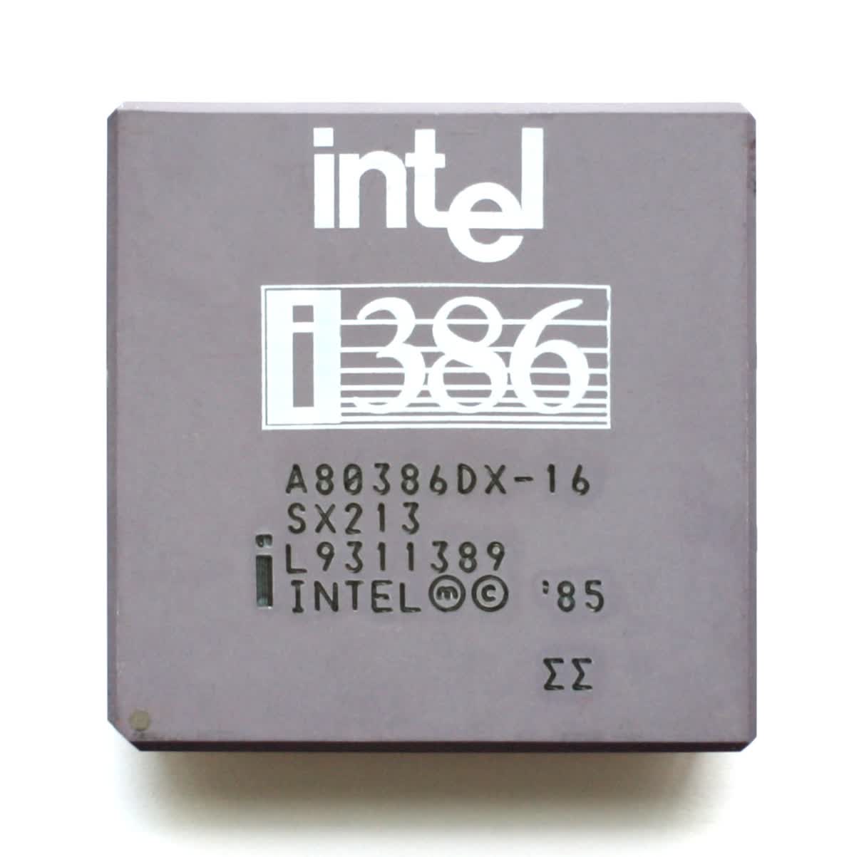
Intel 80386DX с частотой 16МГц (1985).
Целое (Integer) – в математике, это такое число, которое не имеет дробной части. Например, 8 или -12. Процессоры типа интеловского 80386SX не имели врожденной способности сложить, скажем, 3.80 и 7.26 – такие дробные числа называются числами с плавающей точкой (или запятой, в русском языке это без разницы) – по-английски FP, floating point или просто floats. Чтобы справиться с ними, нужен был другой процессор, например 80387SX, и отдельный набор инструкций – список команд, который сообщает процессору, что делать.
В те времена под инструкциями x86 понимали наборы команд для целочисленных (integer) операций, а под инструкциями x87 – для чисел с плавающей точкой (float). В наши дни все операции умеет выполнять один процессор, поэтому мы используем термин x86 для обозначения набора инструкций обоих типов данных.
Использование отдельных сопроцессоров для обработки разных типов данных было нормой, пока Intel не представила 80486: их первый CPU для персоналок со встроенным математическим сопроцессором для обработки вещественных данных (FPU, Floating Point Unit).
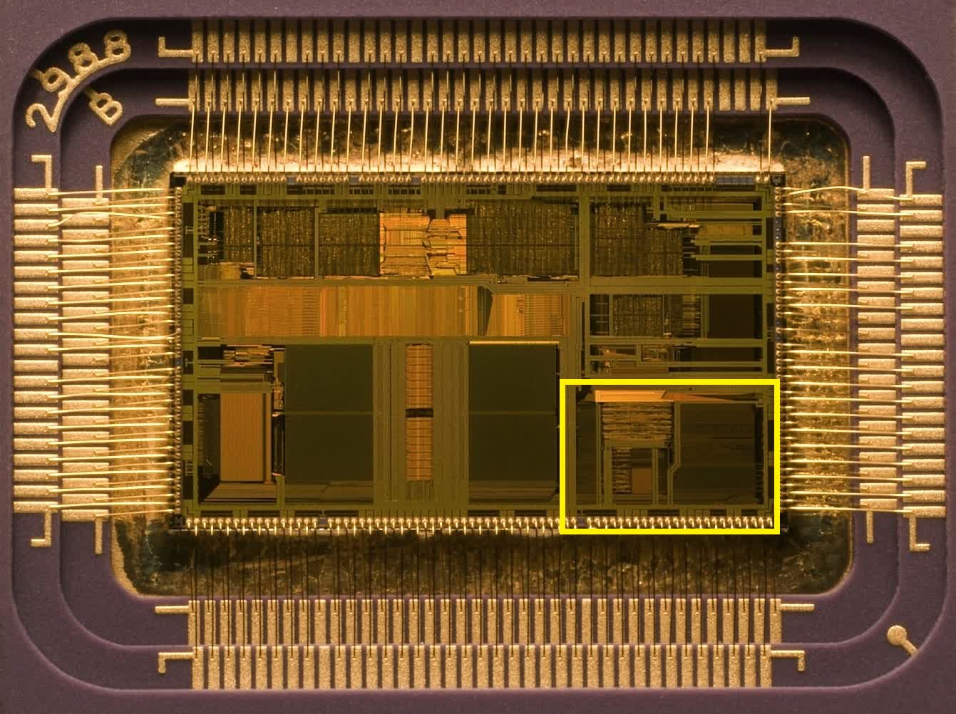
Intel 80486: Жёлтым цветом выделен блок FPU для обработки чисел с плавающей точкой.
Как вы можете видеть, этот блок совсем немного занимает места в процессоре, но рывок в производительности, благодаря этому решению, был огромен.
Но в целом принцип работы оставался скалярным, и таким он перешел и к преемнику 486-го: оригинальному Intel Pentium.
И пройдёт ещё три года после релиза этого первого Пентиума, прежде чем Intel представит миру Pentium MMX. Это произошло в октябре 1996 года.
V – значит «векторный». А MMX что значит?
В мире математики числа можно группировать в наборы различных видов и размеров – одна такая упорядоченная совокупность называется арифметическим вектором. Проще всего представить его себе в виде списка значений, расположенных горизонтально или вертикально. Технология MMX привнесла в мир процессоров возможность выполнять векторные математические вычисления.
Однако она была изначально довольно ограниченной, поскольку оперировала только целыми числами и фактически эксплуатировала для своих целей регистры FPU. Поэтому программисты, желающие использовать какие-то инструкции MMX, вынуждены иметь в виду, что при выполнении таких инструкций любые вычисления с плавающей запятой не могут выполняться одновременно с ними.
Знаменитая реклама технологии Intel MMX (1997).
FPU Pentium имел 64-битные регистры, и в операциях MMX каждый из них мог вместить два 32-битных, четыре 16-битных или восемь 8-битных целых числа. Именно эти группы чисел и являются векторами, и каждая инструкция, предназначенная для них, будет выполняться сразу над всеми значениями в группе.
Такой принцип получил название SIMD (single instruction, multiple data, «одиночный поток команд, множественный поток данных») и знаменует собой большой шаг вперед в развитии возможностей процессоров для персональных компьютеров.
Ну а какие приложения выигрывают от использования такого принципа? Практически все, которым приходится выполнять одинаковые вычисления над группой однородных данных, и в первую очередь это некоторые функции в 3D-моделировании и мультимедийных технологиях, а также в системах обработки стандартных сигналов.
Например, MMX можно применить для ускорения умножения матриц при обработке вершин в 3D, или для смешивания видеопотоков при работе с хромакеем или альфа-композитингом.

Процессор AMD K6-2 – где-то там есть 3DNow!
К сожалению, внедрение MMX продвигалось довольно медленными темпами из-за негативного влияния этой технологии на производительность операций с плавающей точкой. AMD частично решила эту проблему, создав свою собственную версию под названием 3DNow! примерно через два года после появления MMX. Технология от AMD предлагала больше инструкций SIMD и умела обрабатывать числа с плавающей точкой, но также страдала от недостатка понимания программистами.
Ах, да! Как же официально расшифровывается аббревиатура MMX? Согласно Intel – никак!
Проще пареной SSE
Ситуация переломилась в лучшую сторону с приходом в 1999 году процессора Intel Pentium III. Он принёс с собой блестящую реализацию векторной функции под названием SSE (Streaming SIMD Extensions, «потоковые расширения SIMD»). На этот раз это был дополнительный набор из восьми 128-битных регистров, отдельных от регистров в FPU, и стек дополнительных инструкций для обработки чисел с плавающей точкой.
Использование независимых регистров означает, что больше нет такой сильной зависимости от FPU, хотя Pentium III не мог выполнять инструкции SSE одновременно с инструкциями FP. А также, новая функция поддерживает только один тип данных в регистрах: четыре 32-битных FP-числа.
Но переход к использованию FP-инструкций SIMD позволил значительно увеличить производительность в таких приложениях, как кодирование/декодирование видео, обработка изображений и звука, сжатие файлов и многих других.
Pentium IV: желтым цветом выделен блок регистров SSE2.
Усовершенствованная версия SSE2 появилась в 2001 году вместе с Pentium 4, и на этот раз поддержка типов данных была намного лучше: четыре 32-битных или два 64-битных FP-числа, а также шестнадцать 8-битных, восемь 16-битных, четыре 32-битных или два 64-битных целых числа. Регистры MMX остались в процессоре, но все операции MMX и SSE могли выполняться с использованием независимых 128-битных регистров SSE.
Модификация SSE3 появилась на свет в 2003 году, имея больше инструкций и возможность выполнять некоторые математические вычисления между значениями внутри одного регистра.
Ещё через 3 года мы познакомились с архитектурой Intel Core, принёсшей ещё одну ревизию технологии SIMD (SSSE3 – Supplemental SSE, «расширенные SSE»), и чуть позже в том же году – финальную версию, SSE4.
В 2007 году AMD применила собственную версию расширений CPU-инструкций SSE4 в своей архитектуре Barcelona. С названием в AMD париться не стали, и назвали свою версию просто SSE4a.
С линейкой Nehalem Core в 2008 году было выпущено незначительное обновление этой версии, которую Intel обозначила как SSE4.2 (а под SSE4.1 стали понимать исходную версию этого обновления). Обновления не затронули регистры, а лишь добавили больше инструкций в таблицу, расширив диапазон возможных математических и логических операций.
AMD, со своей стороны, сперва предложила новую версию SSE5, но позже решила разделить ее на три отдельных расширения, одно из которых довольно проблемное – подробнее об этом чуть позже.
К концу 2008 года и Intel, и AMD поставляли процессоры, которые уже могли обрабатывать все версии наборов инструкций от MMX до SSE4.2, и многие приложения (в основном игры) начали требовать этих функций для работы.
Время для новых букв
2008 год также был годом, когда Intel объявила о том, что они работают над значительным апгрейдом своей системы SIMD, и в 2011 году выкатила линейку процессоров Sandy Bridge с поддержкой набора инструкций AVX (Advanced Vector Extensions, «продвинутые векторные расширения»).
Всё удвоилось: вдвое больше векторных регистров и вдвое больше их размер.
Шестнадцать 256-битных регистров вмещают только восемь 32-битных или четыре 64-битных вещественных числа, поэтому в плане форматов данных, этот набор инструкций более ограничен в сравнении с SSE, но ведь и SSE никто не отменял. К тому времени программная поддержка векторных операций для CPU была уже хорошо отлажена, начиная с фундаментального мира компиляторов, заканчивая сложными приложениями.
И не даром: Core i7-2600K (или подобный ему), работающий на частоте 3,8ГГц, потенциально может выдавать более 230 GFLOPS (миллиардов операций с плавающей точкой в секунду) при выполнении инструкций AVX – неплохо для дополнения, относительно немного места занимающего на кристалле процессора.
Или могло бы быть неплохо, если бы он действительно работал на частоте 3,8ГГц. Частично проблема AVX заключалась в том, что нагрузка на чип получалась настолько высокой, что Intel пришлось заставить процессор автоматически снижать тактовую частоту в этом режиме примерно на 20%, чтобы уменьшить энергопотребление и не допустить перегрева. К сожалению, такова цена за выполнение любой работы SIMD в современном процессоре.
Еще одно усовершенствование, предлагаемое в AVX – это возможность работать одновременно с тремя значениями. Во всех версиях SSE операции выполнялись между двумя значениями, после чего результат заменял одно из них в регистре. При выполнении инструкций SIMD AVX не трогает исходные значения, сохраняя результирующее значение в отдельный регистр.
AVX2 был выпущен вместе с архитектурой Haswell для процессоров Core 4-го поколения в 2013 году, и представлял собой довольно значительный апгрейд, благодаря добавлению нового расширения: FMA (Fused Multiply-Add, «умножение-сложение с однократным округлением»).
Эта независимая функция в составе AVX2 была крайне востребована для приложений, работающих с векторной и матричной математикой, поскольку давала возможность выполнять две операции с помощью одной инструкции. Функция поддерживала и скалярные операции также.
Проблема оказалась в том, что FMA от Intel отличался от аналогичного расширения AMD настолько, что они были совершенно несовместимы. Причина в том, что Intel FMA представляет собой систему с тремя операндами, то есть работает с тремя отдельными значениями: два слагаемых и сумма, либо три слагаемых и сумма, замещающая одно из слагаемых.
У версии от AMD четыре операнда, поэтому она может вычислить 3 числа и записать ответ в отдельный регистр, не трогая исходные значения. Математически FMA4 лучше, чем FMA3, но его реализация немного сложнее, как с точки зрения программирования, так и с точки зрения интеграции функции в процессор.
AVX-512: а не многовато-ли?
AVX2 ещё только начал появляться на рынке процессоров, а Intel уже плела маниакальные планы относительно его преемника, AVX-512, и общий настрой среди разработчиков был такой: «больше регистров богу регистров!». Мало того, что этих самых регистров снова вдвое больше, и они снова вдвое увеличились в размере, так ещё и появился стек новых инструкций и поддержка устаревших.
Первой партией чипов, на которых поднялся в воздух набор функций AVX-512, стала серия Xeon Phi 7200 – второе поколение громоздких и очень многоядерных процессоров Intel, ориентированных на рынок суперкомпьютеров.
72-ядерный 288-потоковый Knights Landing Xeon Phi.
В отличие от всех предыдущих реализаций, новый набор векторных инструкций состоял из 19-и компонентов: базового – AVX-512F, – необходимого для обеспечения совместимости, и множества весьма специфических. Эти дополнительные наборы охватывают такие области операций, как обратная математика, целочисленные FMA и алгоритмы свёрточной (конволюционной) нейронной сети (CNN-алгоритмы).
Первоначально AVX-512 был только прерогативой крупнейших чипов Intel, предназначенных для рабочих станций и серверов, но теперь их недавние архитектуры Ice Lake и Tiger Lake также поддерживают его. Да, не удивляйтесь: вы можете купить легкий ноутбук с процессором, имеющим 512-битные векторные блоки.
Это может показаться круто. А может и не показаться – в зависимости от вашей точки зрения. Регистры на кристалле CPU обычно группируются в так называемом регистровом файле, как видно на макрофото ниже.
2-ядерный Intel Skylake
Желтым прямоугольником выделен файл векторных регистров, красный прямоугольник – это наиболее вероятное расположение файла целочисленного регистра. Обратите внимание, насколько файл векторного регистра больше integer-регистра. В Skylake используются 256-битные регистры AVX2, следовательно аналогичный векторный регистровый файл AVX-512 занял бы на таком же кристалле в четыре раза больше места: вдвое больше, потому что вдвое больше их размер, и ещё вдвое – потому что самих регистров вдвое больше.
А очень-ли нужно такое количество векторных регистров маленькому чипу, который должен быть максимально мобильным? Хоть речь и не о лишних килограммах в ноутбуке, а лишь о небольшой части площади ядра процессора, каждый квадратный миллиметр имеет значение, когда речь идет о миниатюризации мобильных устройств и наиболее эффективном использовании доступного пространства в них.
И учитывая, что использование AVX в любом виде приводит к автоматическому уменьшению тактовой частоты, использование AVX-512 на таких платформах скорее всего приведет к ещё более сомнительным издержкам по сравнению с любым из своих предшественников, поскольку при работе он потребляет еще больше энергии.
И проблема AVX-512 не только в применении к небольшим мобильным процессорам. Разработчикам, пишущим код для работы на рабочих станциях и серверах, и для которых увеличение возможностей векторных расширений действительно важный вопрос, потребуется создавать несколько версий кода. Это связано с тем, что не все процессоры с AVX-512 работают с одинаковым набором команд.
Например, набор IFMA (Integer Fused Multiply Add, «целочисленное умножение-сложение с однократным округлением») доступен только на процессорах Cannon, Ice и Tiger Lake. В то время как процессоры на архитектуре Cooper и Cascade Lake его не поддерживают, несмотря на то, что они относятся к сегменту процессоров для серверов и рабочих станций.
Стоит отметить, что AMD не предлагает поддержку AVX-512, и не собирается. По их мнению, обработка массивных векторных вычислений – это прерогатива GPU. С AMD полностью солидарна Nvidia, и обе компании уже выпустили продукты специально для таких нужд.
И дальше что?
Много лет назад процессор с возможностью обработки векторной математики ознаменовал собой эпохальный прорыв. Современные процессоры обладают огромными возможностями, предлагая множество наборов инструкций для обработки целочисленных операций и операций с плавающей запятой для скалярных, векторных и матричных данных.
Что касается последних двух типов данных, то CPU теперь напрямую конкурируют с GPU: ведь мир 3D-графики – это как раз всё, что связано с SIMD, векторами, плавающими точками и т.д. И производители GPU не спали – разработка графических ускорителей велась стремительными темпами. В начале 2010-х годов купить видеокарту, процессор которой способен выполнять почти 800 миллиардов инструкций SIMD в секунду, вы уже могли менее чем за 500 долларов.
Это больше, чем то, на что сейчас способны лучшие из десктопных CPU. Но они и не предназначены для рекордов в какой-то конкретной области – их задача обрабатывать очень обобщенный код, который зачастую не повторяется или легко распараллеливается. Поэтому, не стоит думать, что возможности SIMD столь жизненно-важны для CPU, скорее это полезное дополнение к его арсеналу.

Вас интересует производительность SIMD в чистом виде? Ваш выбор – видеокарта, а не материнка!
Стремительное развитие графических процессоров недвусмысленно намекает, что для CPU нет нужды иметь чересчур большие векторные блоки, и почти наверняка именно поэтому AMD даже не пыталась разрабатывать своего собственного преемника для AVX2 (расширение, которое они используют в своих чипах с 2015 года). Давайте также не будем забывать, что процессоры следующего поколения могут больше походить на мобильные однокристальные (SoC, System-on-a-Chip), где под каждый тип задач выделена площадь на кристалле. Intel, в свою очередь, похоже, стремится внедрить AVX-512 в как можно большее количество продуктов.
Ждёт ли нас ещё и AVX-1024? Вряд ли, либо очень нескоро. Скорее всего, Intel займётся расширением AVX-512 с помощью дополнительных компонентов с инструкциями, чтобы повысить гибкость, а чистую SIMD-производительность переложит на плечи своей недавно разработанной линейки графических процессоров Xe.
Библиотеки SSE и AVX теперь являются неотъемлемой частью программного обеспечения: Adobe Photoshop требует, чтобы процессоры поддерживали как минимум SSE4.2; API машинного обучения TensorFlow требует поддержки AVX; Microsoft Teams может выполнять фоновые видеоэффекты, только если доступен AVX2.
Это говорит только об одном: несмотря на то, что в плане обработки SIMD графическим процессорам нет равных, этот функционал ещё долго будет в арсенале CPU. Так что будем ждать нового поколения векторных расширений и надеюсь, реклама нас впечатлит.
Процессор — сердце любого компьютера. Мы знаем, как он выглядит снаружи. Но интересно же — как он выглядит изнутри?

Процессор состоит из миллиардов транзисторов сопоставимых по размеру с молекулой ДНК. Действительно размер молекулы ДНК составляет 10 нм. И это не какая-то фантастика! Каждый день процессоры помогают нам решать повседневные задачи. Но вы когда-нибудь задумывались, как они это делают? И как вообще люди заставили кусок кремния производить за них вычисления?
Сегодня мы разберем базовые элементы процессора и на практике проверим за что они отвечают. В этом нам поможет красавец-ноутбук — Acer Swift 7 с процессором Intel на борту.
Ядро процессора
Модель нашего процессора i7-1065G7. Он четырёхядерный и ядра очень хорошо видны на фотографии.

Каждое ядро процессора содержит в себе все необходимые элементы для вычислений. Чем больше ядер, тем больше параллельных вычислений процессор может выполнять. Это полезно для многозадачности и некоторых ресурсоемких задач типа 3D-рендеринга.
Например, для теста мы одновременно запустили четыре 4К-видео. Нагрузка на ядра рспределяется более менее равномерно: мы загрузили процессор на 68%. В итоге больше всего пришлось переживать за то хватит ли Интернет-канала. Современные процессоры отлично справляются с многозадачностью.
Почему это важно? Чтобы ответить на этот вопрос, давайте разберемся — как же работает ядро?
По своей сути ядро — это огромный конвейер по преобразованию данных. На входе загружаем одно, на выходе получаем другое. В его основе лежат транзисторы. Это миниатюрные переключатели, которые могут быть в всего в двух состояниях: пропускать ток или нет. Эти состояния компьютер интерпретирует как нули и единицы, поэтому все данные в компьютере хранятся в двоичном коде.
Можно сказать, что компоненты внутри компьютера общаются между собой при помощи подобия Азбуки Морзе, которая тоже является примером двоичного кода. Только компьютер отстукивает нам не точки и тире, а нолики и единички. Казалось бы, вот есть какой-то переключатель, и что с ним можно сделать? Оказывается очень многое!
Если по хитрому соединить несколько транзисторов между собой, то можно создать логические вентили. Это такие аналоговые эквиваленты функции “если то”, ну как в Excel. Если на входе по обоим проводам течет ток, то на выходе тоже будет течь или не будет или наоборот, вариантов не так уж и много — всего семь штук.
Но дальше комбинируя вентили между собой в сложные аналоговые схемы, мы заставить процессор делать разные преобразования: складывать, умножать, сверять и прочее.
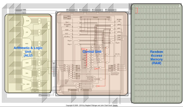
Поэтому ядро процессора состоит из множества очень сложных блоков, каждый из которых может сделать с вашими данными что-то своё.
Прям как большой многостаночный завод, мы загружаем в него сырье — наши данные. Потом всё распределяем по станкам и на выходе получаем результат.
Но как процессор поймёт, что именно нужно делать с данными? Для этого помимо данных, мы должны загрузить инструкции. Это такие команды, которые говорят процессору:
- это надо сложить,
- это перемножить,
- это просто куда-нибудь отправить.
Инструкций очень много и для каждого типа процессора они свои. Например, в мобильных процессорах используется более простой сокращённый набор инструкций RISC — reduced instruction set computer.
А в ПК инструкции посложнее: CISC — complex instruction set computer.
Поэтому программы с мобильников не запускаются на компах и наоборот, процессоры просто не понимают их команд. Но чтобы получить от процессора результат недостаточно сказать — вот тебе данные, делай то-то. Нужно в первую очередь сказать, откуда брать эти данные и куда их, собственно, потом отдавать. Поэтому помимо данных и инструкций в процессор загружаются адреса.
Память
Для выполнения команды ядру нужно минимум два адреса: откуда взять исходные данные и куда их положить.
Всю необходимую информацию, то есть данные, инструкции и адреса процессор берёт из оперативной памяти. Оперативка очень быстрая, но современные процессоры быстрее. Поэтому чтобы сократить простои, внутри процессора всегда есть кэш память. На фото кэш — это зелёные блоки. Как правило ставят кэш трёх уровней, и в редких случаях четырёх.
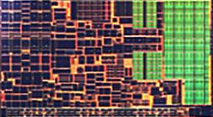
Самая быстрая память — это кэш первого уровня, обозначается как L1 cache. Обычно он всего несколько десятков килобайт. Дальше идёт L2 кэш он уже может быть 0,5-1 мб. А кэш третьего уровня может достигать размера в несколько мегабайт.

Правило тут простое. Чем больше кэша, тем меньше процессор будет обращаться к оперативной памяти, а значит меньше простаивать.
В нашем процессоре кэша целых 8 мб, это неплохо.
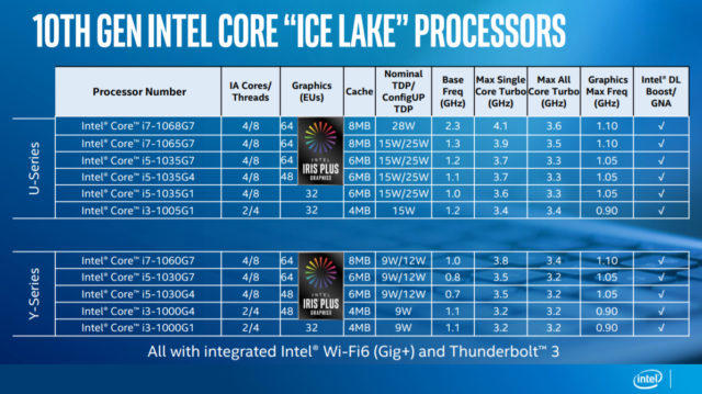
Думаю тут всё понятно, погнали дальше.
Тактовая частота
Если бы данные в процессор поступали хаотично, можно было бы легко запутаться. Поэтому в каждом процессоре есть свой дирижёр, который называется тактовый генератор. Он подает электрические импульсы с определенной частотой, которая называется тактовой частотой. Как вы понимаете, чем выше тактовая частота, тем быстрее работает процессор.
Занимательный факт. По-английски, тактовая частота — это clock speed. Это можно сказать буквальный термин. В компьютерах установлен реальный кристалл кварца, который вибрирует с определенной частотой. Прямо как в наручных кварцевых часах кристалл отсчитывает секунды, так и в компьютерах кристалл отсчитывает такты.
Обычно частота кристалла где-то в районе 100 МГц, но современные процессоры работают существенно быстрее, поэтому сигнал проходит через специальные множители. И так получается итоговая частота.
Современные процессоры умеют варьировать частоту в зависимости от сложности задачи. Например, если мы ничего не делаем и наш процессор работает на частоте 1,3 ГГц — это называется базовой частотой. Но, к примеру, если архивируем папку и мы видим как частота сразу увеличивается. Процессор переходит в турбо-режим, и может разогнаться аж до 3,9 ГГц. Такой подход позволяет экономить энергию, когда процессор простаивает и лишний раз не нагреваться.
А еще благодаря технологии Intel Hyper-threading, каждое ядро делится на два логических и мы получаем 8 независимых потоков данных, которые одновременно может обрабатывать компьютер.
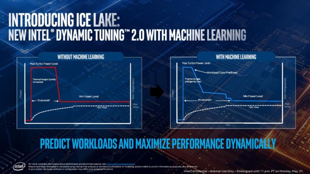
Что прикольно, в новых процессорах Intel скорость частот регулирует нейросеть. Это позволяет дольше держать турбо-частоты при том же энергопотреблении.
Вычислительный конвейер
Так как ядро процессора — это конвейер, все операции через стандартные этапы. Их всего четыре штуки и они очень простые. По-английски называются: Fetch, Decode, Execute, Write-back.
- Fetch — получение
- Decode — раскодирование
- Execute — выполнение
- Write-back — запись результата

Сначала задача загружается, потом раскодируется, потом выполняется и, наконец, куда-то записывается результат.
Чем больше инструкций можно будет загрузить в конвейер и чем меньше он будет простаивать, тем в итоге будет быстрее работать компьютер.
Предсказатель переходов
Чтобы конвейер не переставал работать, инженеры придумали массу всяких хитростей. Например, такую штуку как предсказатель переходов. Это специальный алгоритм, который не дожидаясь пока в процессор поступит следующая инструкция её предугадать. То есть это такой маленький встроенный оракул. Вы только дали какую-то задачу, а она уже сделана.
Такой механизм позволяет многократно ускорить систему в массе сценариев. Но и цена ошибки велика, поэтому инженеры постоянно оптимизируют этот алгоритм.
Микроархитектура
Все компоненты ядра, как там всё организовано, всё это называется микроархитектурой. Чем грамотнее спроектирована микроархитектура, тем эффективнее работает конвейер. И тем больше инструкций за такт может выполнить процессор. Этот показатель называется IPC — Instruction per Cycle.
А это значит, если два процессора будут работать на одинаковой тактовой частоте, победит тот процессор, у которого выше IPC.
В процессорах Ice Lake, Intel использует новую архитектуру впервые с 2015 года. Она называется Sunny Cove.
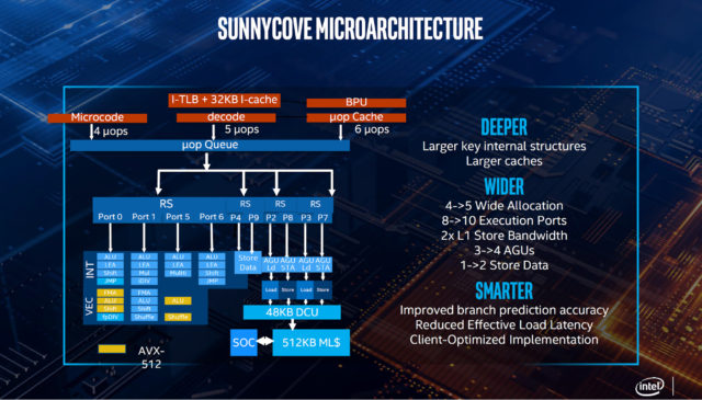
Показатель IPC в новой архитектуре аж на 18% на выше чем в предыдущей. Это большой скачок. Поэтому при выборе процессора обращаете внимание, на поколение.
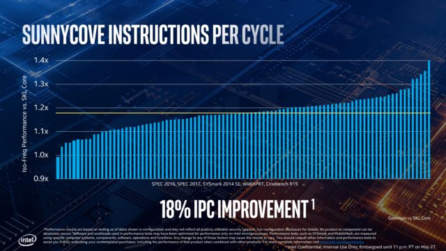
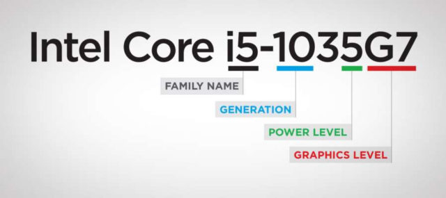
Система на чипе
Естественно, современные процессоры — это не только центральный процессор. Это целые системы на чипе с множеством различных модулей.
ГП
В новый Intel больше всего места занимает графический процессор. Он работает по таким же принципам, что и центральный процессор. В нём тоже есть ядра, кэш, он тоже выполняет инструкции. Но в отличие от центрального процессора, он заточен под только под одну задачу: отрисовывать пиксели на экране.
Поэтому в графический процессорах ядра устроены сильно проще. Поэтому их даже называют не ядрами, а исполнительными блоками. Чем больше исполнительных блоков тем лучше.
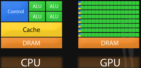
В десятом поколении графика бывает нескольких типов от G1 до G7. Это указывается в названии процессора.
А исполнительных блоков бывает от 32 до 64. В прошлом поколении самая производительная графика была всего с 24 блоками.
Также для графики очень важна скорость оперативки. Поэтому в новые Intel завезли поддержку скоростной памяти DDR4 с частотой 3200 и LPDDR4 с частотой 3733 МГц.
У нас на обзоре ноутбук как раз с самой топовой графикой G7. Поэтому, давайте проверим на что она способна! Мы проверили его в играх: CS:GO, Dota 2 и Doom Eternal.
Что удобно — Intel сделали портал gameplay.intel.com, где по модели процессора можно найти оптимальные настройки для большинства игр.
В целом, в Full HD разрешении можно комфортно играть в большинство игр прямо на встроенной графике.

Thunderbolt
Но есть в этом процессоре и вишенка на торте — это интерфейс Thunderbolt. Контроллер интерфейса расположен прямо на основном кристалле, вот тут.
Такое решение позволяет не только экономить место на материнской плате, но и существенно сократить задержки. Проверим это на практике.

Подключим через Thunderbolt внешнюю видеокарту и монитор. И запустим те же игры. Теперь у нас уровень производительности ноутбука сопоставим с мощным игровым ПК.
Но на этом приколюхи с Thunderbolt не заканчиваются. К примеру, мы можем подключить SSD-диск к монитору. И всего лишь при помощи одного разъёма на ноуте мы получаем мощный комп для игр, монтажа и вообще любых ресурсоемких задач.
Мы запустили тест Crystalmark. Результаты вы видите сами.
Но преимущества Thunderbolt на этом не заканчиваются. Через этот интерфейс мы можем подключить eGPU, монитор, и тот же SSD и всё это через один кабель, подключенный к компу.

Надеюсь, мы помогли вам лучше разобраться в том, как работает процессор и за что отвечают его компоненты.
Post Views: 17 559